
|

|
Forum Index : Electronics : Various aspects of home brew inverters
| Author | Message | ||||
| poida Guru Joined: 02/02/2017 Location: AustraliaPosts: 1466 |
Mike, I agree, a high quality LP filter is worth considering. I'm not sure we need to go that hard though. Are you suggesting that inverter AC output voltage is not worth monitoring due to core's regulation? In my experience, the transformers I use need a closed loop feedback using output AC voltage. Some figures: test load 150W @ 230V AC DC supply 27V Approx DC supply current 150/27 = 5.5A Primary winding 2 x 6mm2 Secondary winding - whatever Aerosharp specify in their 1500VA toroid I see the pwm duty % increase when I apply the load. This increase is due to the closed loop control. I need to get home to measure the duty cycle % accurately. I find the 1500VA toroid , as well as the 3000VA, to be poorly regulated to such a degree that I need to use a small 9V transformer on the AC output to get an accurate voltage sample. I tried, as others have suggested and tried, to put a few turns around the toroid to get 5V or so and feed that, rectified and scaled as needed, into the EG8010 Fvb or the nanoverter's Vfb input. The output AC voltage drops under small loads (150W) But with Vfb and a representative sample voltage: within 1 volt. wronger than a phone book full of wrong phone numbers |
||||
| Solar Mike Guru Joined: 08/02/2015 Location: New ZealandPosts: 1204 |
Poida, I use the DC battery voltage sample for my feedback input, I'm not using the 1.5/3KVA original cores but custom much bigger, which must have better regulation, so I guess for the lighter cores then its appropriate to keep using the original AC derived signal; I also use the same battery sample for shut down if it gets too low. (below set limit for 10 seconds) Cheers Mike |
||||
| poida Guru Joined: 02/02/2017 Location: AustraliaPosts: 1466 |
I have developed far better mains sync code. Now it stays within +/- 2 counts of the sync setpoint. It uses PD control (like PID control but no Integral component) There is 400 counts per 50 Hz waveform so it's +/- 1.8 degrees It can obtain sync from about 40 to 58 Hz and it syncs up less than 1/2 second. This is the way to go. I will post video of it's performance and code later. wronger than a phone book full of wrong phone numbers |
||||
| tinyt Guru Joined: 12/11/2017 Location: United StatesPosts: 558 |
I think it is better to directly sense the AC output. This way the code can react if there is deterioration in the power mosfet bridge circuit like connections to the toroid primary becoming partially loose, etc. Attached is revised schematic for review/comments. 2018-11-20_142450_NANOVERTERdraft6.pdf Note for C3 and jumper and active low pass filter are added. Maybe active low pass filter should be used only on critical analogs. This will save on parts and pcb size. |
||||
| Tinker Guru Joined: 07/11/2007 Location: AustraliaPosts: 1904 |
Thanks poida, for explaining the frequency stability of the nano. I'm sure its my frequency meter, you do have much better gear on your workbench. If I was any good at programming I would check your code if I have 799 or 800 in my downloaded version. As it is - I better leave that part alone  . .Since you are logging the mains frequency already perhaps, once you have a nano driven inverter powering your house, logging its frequency could be done too? If there are only short term drifts up & down, like the mains, its not a big deal. But if the nano's frequency drifts continually in the same direction there would be a time it might require correction somehow. Tinyt, can I ask you a big favor please? Could you do away with the decimal point at component values in your excellent schematics? It has a habit to be missed by tired eyes. So, instead of quoting 4.7K just write 4K7 (4R7, 4M7 etc). This is generally preferred anyway. Ditto with capacitors if doable (4.7uF = 4u7) Klaus |
||||
| poida Guru Joined: 02/02/2017 Location: AustraliaPosts: 1466 |
Here is info on my test inverter. 1500VA Aerosharp toroid, 2 x 6mm2 primary winding. 27.6 V DC supply, 2 x 6A bench power supplies connected in parallel, then this into 2 x 100AH 12V SLA in series. This is a sizable supply for 6 Amp load. Idle, duty cycle % is 63.6% under load, 150W, 66.7 % DC amps 6.6A The power supplies maintain constant voltage, increasing current as needed. I still think I will use AC output for Vfb. We use what works for our own systems. wronger than a phone book full of wrong phone numbers |
||||
| wiseguy Guru Joined: 21/06/2018 Location: AustraliaPosts: 1280 |
TinyT, something quite minor, net 1VS is missing from U2 pin 11. I assume all the unused pins on the nano have internal pullup/downs as required ? Perhaps pin 11 should have a pull down in case of input disconnect, will fail safe. (or is there an internal pull down ?) Rest looks good. I still dont get what is happening with the buss wires on the PDF's I have tried 4 different PDF viewers and none show me the bussed wires - I now give up - I dont need to see them, just not sure why I cant. If at first you dont succeed, I suggest you avoid sky diving.... Cheers Mike |
||||
| tinyt Guru Joined: 12/11/2017 Location: United StatesPosts: 558 |
Thanks wiseguy, that missing 1VS net is not a minor mistake. I don't intend to manually route the pcb, it will take me forever to do it. I will be using spectra autorouter and if that net name is not there, U2 pin 11 will not be connected to the 1VS net. The IR21844 data sheet typical connection does not show an external pull down on the VS pin, but I added them (2 resistors won't occupy much space and just don't install if not needed). I think I now understand the missing bus wires that you are looking for, look at the ribbon connector pins (wide blue lines?). Are they the ones? If they are, I did not add them as the drawing now is crammed and busy. Attached is the revised schematic for review/comment. 2018-11-21_005308_NANOVERTERdraft7.pdf. I also removed decimal points on values as requested by tinker. |
||||
| Tinker Guru Joined: 07/11/2007 Location: AustraliaPosts: 1904 |
This is coming along very nicely, thanks to all who put so much of their time into this project. I think I got that external syncing sorted in my head but please correct me if I'm wrong. So lets assume I have my nano controlled inverter up and running, powering my house. Its a cloudy day and the battery bank is being drained too much. I fire up the generator and when its running connect 12V AC from it (via an isolation transformer) to connector J1. The mains output from the generator goes to a relay box which has two relays with 20Amp rated contacts (I would switch both, active & neutral). One side of the N/O contacts go to the house AC wiring. The other side to the generator AC output. When I open the jumper (JP1) the nano syncs to the generator, which becomes the master power source since its frequency is fixed. Once both are synced relay K1 activates and connects the generator output to the house supply. If the house requires less power than the generator can supply then the excess back charges the battery bank via the inverter. Just as now happens at my place with solar panels and a grid tie inverter that runs stand alone. If this is correct I'm sure there are others here that would find this feature very useful. Klaus |
||||
| Zibe Newbie Joined: 15/01/2018 Location: AustraliaPosts: 10 |
I have added a separate topic for adding WIFI as mentioned before: https://www.thebackshed.com/forum/forum_posts.asp?TID=10920&PN=1&TPN=1 Its very easy to upto add 8 tags of data every 30 seconds over serial. Integrating the code on the arduino side is as simple an example from my inverter code: void ThingSpeakString(void) { // Generates a formatted ThingSpeak String of the data if ((millis() - preMilliSec_SerialData ) > intervalSerialDataUpdate) { Serial.begin(9600); Serial.print(F("&1=")); //Field 1: Voltage Serial.print(supVoltage, 1); Serial.print(F("&2=")); //Field 2: Current Serial.print(supCurrent, 1); Serial.print(F("&3=")); //Field 3: Power Serial.print(supPower,0); Serial.print(F("&4=")); //Field 4: Energy Serial.print(totalPowerConsumption / 1000, 2); Serial.print(F("&5=")); //Field 5: Temperature Serial.print(heatSinkTemp, 1); Serial.print(F("&6=")); //Field 6: Amplitude Serial.print(DataSetPosition8200, 2); Serial.print(F("~")); Serial.end(); preMilliSec_SerialData = millis(); // Update when the serial data was last sent } |
||||
| poida Guru Joined: 02/02/2017 Location: AustraliaPosts: 1466 |
Tinker: I think you have it 100% right. There will be other ways to make use of this, I suspect. I want the sync function to be used for off-grid systems where another AC source may be running. Small differences in phase angle will produce large bi-directional current flows. I would expect to see those who try to use this, to install suitable contact breakers and fast acting relays to control & protect the nanoverter's AC output. Right now, I picture spectacular consequences from missteps from early adopters. wronger than a phone book full of wrong phone numbers |
||||
renewableMark Guru Joined: 09/12/2017 Location: AustraliaPosts: 1678 |
Nice work Poida and Tinyt, I'll keep plugging along building my second Madinverter and when final version of your design is published new control boards will get ordered. I certainly don't want to make any more smoke and destroy a gen and inverter in one hit. Would these parts be suitable? rcbo ssr Cheers Caveman Mark Off grid eastern Melb |
||||
| poida Guru Joined: 02/02/2017 Location: AustraliaPosts: 1466 |
Tinyt: I would like for you to add an opto coupler between the AC sync output and D2. I found in testing that there was so much noise, the voltage divided sample of the AC sync contained huge spikes from the PWM. These spikes upset the edge trigger of INT0 to a large amount. The source of the noise is numerous poorly routed ground wires, ground loops, un-shielded wires everywhere, and your-guess-is-as-good-as-mine ground reference. pink is INT0 trigger Dark Blue is AC sync volts into D2 (INT0) Light Blue is street AC Yellow is nanoverter AC, if present First is sync'd up, AC sample voltage into pin D2 This is how I developed the sync code, using v1 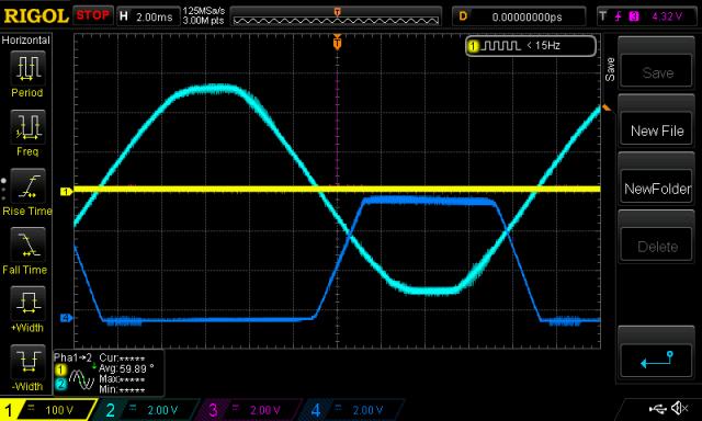 next is with the inverter ON. Noise... Notice the horizonal shift in trigger point, the center line. And so much vertical hash on the input. 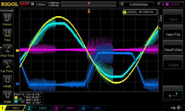 v1 code could barely run, v2 with PID control was unstable. When testing v2 PID sync code with a clean trigger signal, all was OK. But once you switch the inverter on, things go bad. Now with the optocoupler (TLP523-2, something I had handy) Inverter OFF, clean and fast trigger signal, eh? 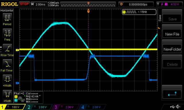 I used the 10cm long earth leads for the DSO probes for the first 3 images. These CRO probe earth leads are well know to be good antennas at RF, and add about 5uH to the measurement too. On the last one, I used the tiny spring wire earth to minimise the RF uptake. I placed the earth wire on pin 5 and the probe tip on pin6 of the TLP523-2. This is the lowest noise probe method I can achieve and closely reflects what the uC sees on it's pin. One inch leads connect the opto's outputs to ground and pin D2 - which probably pick up some noise. And with the inverter ON. No hash on the trigger input, and no time offset added from false triggers on the hash. 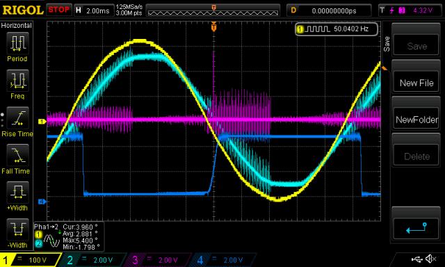 I will adjust the PID setpoint for sync, to align the inverter output to sync input later tonight. I think we will have a challenging fight against noise on all the inputs of our project. Maybe I have won round 1. wronger than a phone book full of wrong phone numbers |
||||
| Solar Mike Guru Joined: 08/02/2015 Location: New ZealandPosts: 1204 |
Poida, it take some design experience to get earthing correct, main thing is to keep all high current earths isolated from analog signal earth, if they have to be linked then it should be a single wire connection to the power section, on the pcb designer layout this is normally shown as a 0R resistor to keep the nets separated. I now use opto coupled drivers to all quadrants of the H bridge power board, earths are more easily isolated to prevent issues as discovered. Where is Warp, he would have some good ideas for this. Cheers Mike |
||||
| poida Guru Joined: 02/02/2017 Location: AustraliaPosts: 1466 |
Better sync now. I have more robust code. I can not imagine how you could develop code while testing driving an inverter without a decent current limiting power supply. I've lost count how many times it has gone into some spasm with the current limiting light on. Imagine if I had one source only:100Amps of SLA grunt. Anyway, I've been trying to provoke bad behavior with random sync signal connection and disconnection. It all looks good to me. video 1 shows sync on and off, provocation of inverter spasm etc. Light blue is INT0 input White is mains AC Yellow is inverter AC video 2 is the same, but Light Blue is sync lock, low = no lock, 5V = lock. wronger than a phone book full of wrong phone numbers |
||||
| brac321 Regular Member Joined: 30/11/2016 Location: SloveniaPosts: 54 |
Poida, looks very promising, actually very good!  OffGrid 24/7: 250w black mono solar panels 6.4kWp, 1x Midnite Classic 150, 1x MorningStar MPPT 60, battery bank 840 Ah @ 48v, modified LF-8K inverter, DC/DC, hot water harvesting, etc. |
||||
| wiseguy Guru Joined: 21/06/2018 Location: AustraliaPosts: 1280 |
I follow a similar philosophy to Warp when it comes to high power stages and isolate as much as possible from the control board. Although it is unproven at this stage I decided to share my inverter approach to minimise noise from the output stages reaching the control board. My power output stage PCB's (2 required for a full bridge) will have 1 leg of the bridge per PCB Each Leg of the bridge will have 4 x FETs in parallel. The upper FET drive stages each have an isolated 12V supply to power the gate driver ICs which are fed by opto-coupled inputs. Another isolated supply drives both the lower FET driver stages on each PCB as they will share a common Source Battery negative connection, and also have opto-coupled inputs. The opto-couplers for each of the 4 sections of the bridge could be driven by 2 x IR2184's which have internal dead-time on the control PCB. Employing simpler drivers & using cross coupled optos as per Warps favored driving method for each bridge leg will provide both dead-time and high noise immunity. As the 4 x bridge stages all have opto-coupled inputs and their power supplies are each isolated there is no direct electrical connection between the FET bridge PCBs and the control PCB - they are in effect galvanically isolated. The control PCB has the small auxiliary power supply that provides the 3 x 12V isolated supplies. It also contains the nano and other support circuitry as per TinyTs circuit. The only connection from the control board to the Power stage will be a ground connection to reference the battery voltage reading - and of course a high impedance resistor for the +Ve Battery voltage measurement. The result should be a very quiet control board environment with minimal noise pickup. If the output bridge was to go totally feral with fireworks etc nothing can pass through the optos or the isolated supplies to damage the control board. The 2 x output PCBs can be easily swapped out or repaired depending on the damage sustained.. For anyone interested here is the circuit - but use at your own risk, this is not intended as a proven project design - yet. I am waiting until Poidas software and the control PCB circuitry is a bit closer before sending them all out for manufacture. 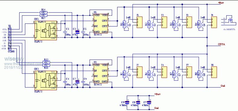 2018-11-22_005206_Output_PCB_Sch.pdf Schematic picture is a bit ordinary so PDF uploaded here If at first you dont succeed, I suggest you avoid sky diving.... Cheers Mike |
||||
| tinyt Guru Joined: 12/11/2017 Location: United StatesPosts: 558 |
Awesome pictures and videos! Here is revised schematic for review/comments. 2018-11-22_011458_NANOVERTERdraft8.pdf I have used the TLP523 since that is the one you used for code development. I also have changed ON_OFF_SIG to ST_SP_SIG (StarT_StoP_SIGnal) to avoid confusion as to what it really does. I have also added a connector for this function. This is in case others want to start with a 'bare-bones' controller and then add the nano2 later. They can plug an external switch to use this function. |
||||
| poida Guru Joined: 02/02/2017 Location: AustraliaPosts: 1466 |
Here is the latest nano1 code, commented to aid in understanding (how much drugs I'm on..) 2018-11-22_081415_nano_1_v3_sync_pid.zip Thanks again Tinyt for the circuit design. Now there is an optocoupler, I think we don't need C3 any more. Maybe we do, only after boards are made and careful DSO probing across C3 will I have any idea if it does anything worthwhile. I like the care given to provide for simple stand alone function. This will be used during testing, by most people. Wiseguy: Nice looking design. wronger than a phone book full of wrong phone numbers |
||||
| tinyt Guru Joined: 12/11/2017 Location: United StatesPosts: 558 |
Hi poida, If nano1 code and IO assignment is complete, can we now continue to nano2 pin assignments? |
||||
| The Back Shed's forum code is written, and hosted, in Australia. | © JAQ Software 2026 |