 |
|
|
|
Site Navigation
Projects & Information
»General Information»Wind turbine Projects »The F&P Smartdrive »Electronic projects »Microcontroller projects »Miscellaneous Kits & Parts
»Basicly Natural Pty Ltd»PVC & Aluminium blades »Scale model farm windmills »Price Watch Discussion Forums
Handy Links
»Wind»Solar »Electric Vehicles »Electronics »Micro Controllers »General Interrest About TheBackShed Getting Started Privacy Policy |
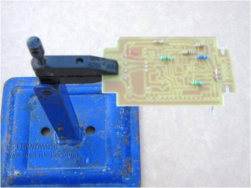
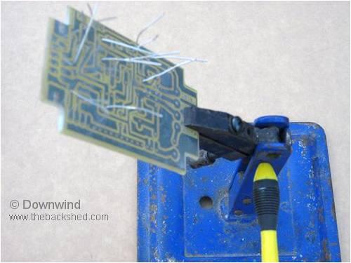
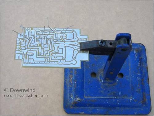
Board assembly As you will all know, one of the awkward things about assembling a board is holding the little bugger while inserting components and soldering. The little helping hands gator clips thingies are more than useless in my experience. There had to be a better way! I fabricated a pivoting clamp that can flip over one way to insert the components and flip back the other way to solder thing in place. It was another project that was well worth the effort and has given many years of service. Have since made several for others and now include a edge around the base to form a tray, as when you unsolder a component for an alteration all those used little bits end up in the tray and ready to be reused again. (or at least found)
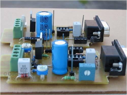
The finished boards
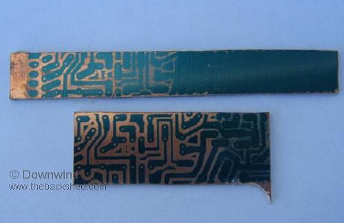
The whole process is a bit rough but it works for me and gives a workable board at the end for minimal effort and cost. The process allows me to produce a reasonable board in less than an hour from printer to assembly and if doing several boards together than this time is reduced greatly per board. You never stop learning with making pcb’s and I hope this helps others to produce fair quality boards of their own. I also hope this inspires others to post their methods of making pcb’s regardless of how simple or complicated the method is. We often use ideas from many sources to find a way that suits our needs best as I have done. What is your method? A few more tips. I think Epson has a much better inkjet ink than canon and others for printing the artwork as it is an alcohol base ink and not water based. It prints sharper edges and is a blacker ink.I use a laser printer now but ink jet was all I had for years. There is no need to wash the board to remove any oil film, as there shouldn’t be any if used correctly. Besides caustic is a great degreaser anyhow. Design software This is a personal choice to most with what they have or know how to use. My preferred choice is ExpressPCB And can be downloaded free from here. ExpressPCB I find its a basic, easy to use software package that can be learnt quickly. Ammonium per-sulphate I use ferric chloride but many etchants will work. If you use ammonium per-sulphate it is a nice clear liquid to work with, but it don’t last as long as ferric chloride. I found mixing ammonium per-sulphate in chlorinated tap water killed it stone dead as an etchant, so use rain water or buy some distilled water. Home made etchant If you don’t have any ferric chloride or any other etchant than a etchant can be made from Hydrogen peroxide ( 3% by volume from the chemist shop or supermarket) and hydrochloric acid (HCL). From bunnings or a hardware store, even a swimming pool place. ( used as a ph adjuster ) Mixed at a ratio of 2 parts hydrogen peroxide to one part neat hydrochloric acid. The solution will turn a redish colour by memory when mixed. ( or was it green??) The life of the solution will only be a few days as it will oxidize quickly and become slow and take all day to etch. Fresh it will work fast and gives a good result. (10 –15 mins ) Copper recovery If you want to recover the copper from a well used lot of ferric chloride before It is discarded, than place a strip of black or uncoated steel sheet metal in the ferric chloride over night. The next day the copper will be crystal like on the bottom and the dark brown ferric chloride will be almost clear hydrochloric acid again. It will not be any good as a etchant after this. Pour the acid off and recover the copper . It is hard to believe, that this dark thick gunk can change so much with the introduction of a bit of steel. Test strip. Keep all the small little offcuts of the pcb sheet to be used as exposure test strips. A test strip is done by exposing an artwork image onto the pcb in stages of time.
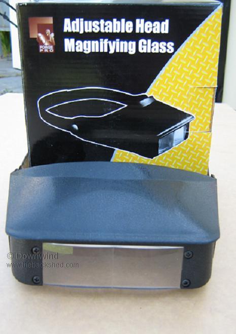
An example is.... Place the artwork on the strip of pcb and expose it for a minute, than place a piece of cardboard over a small portion of the strip one end (10-20mm), expose it again for another minute, then move the cardboard along a little more and expose again for another minute and so on till you run out of pcb strip. Then develop the strip as normal and you will see at what time period of exposure gave the best results. If the test shows over or under exposure through out, than repeat the test and adjust the time period to suit. It is a test well worth doing and is much cheaper than stuffing up a complete board. Once the exposure time is established than it should remain the same, if the same conditions as always used. ( hence why I use a uv scanner method) It dose pay to do a simular test when mixing a fresh batch of caustic solution as I have stripped a board clean in developing with the solution being to strong ( I think I said whoops , bugger and then *%$#@!!) Short cuts never pay!! A good investment is a head set magnifier and once you have one, you will ask yourself how did you made do without it.
The local $2.00 shop “Cheap as Chips” had these out recently for $5.00 . They have a second flip down lense for double magnification ( maybe needed in future years) Well worth the money. ( I bought a $30.00 set a few weeks before these came out and now prefer using the cheap ones.) I can now read those tiny printed part numbers. I am told they work well if you wear glasses, as there is no need to remove your glasses. Funny how fast the soldering becomes when you can see what you are doing. Best get two sets or the misses will steal them for needle threading or whatever?? or the kids may nic them to burn bugs with. (if kids still do that) Pete. Next Page - Some more tips from other contributors. |
||
