
|

|
Forum Index : Electronics : Simple battery charger
| Author | Message | ||||
| larny Guru Joined: 31/10/2011 Location: AustraliaPosts: 349 |
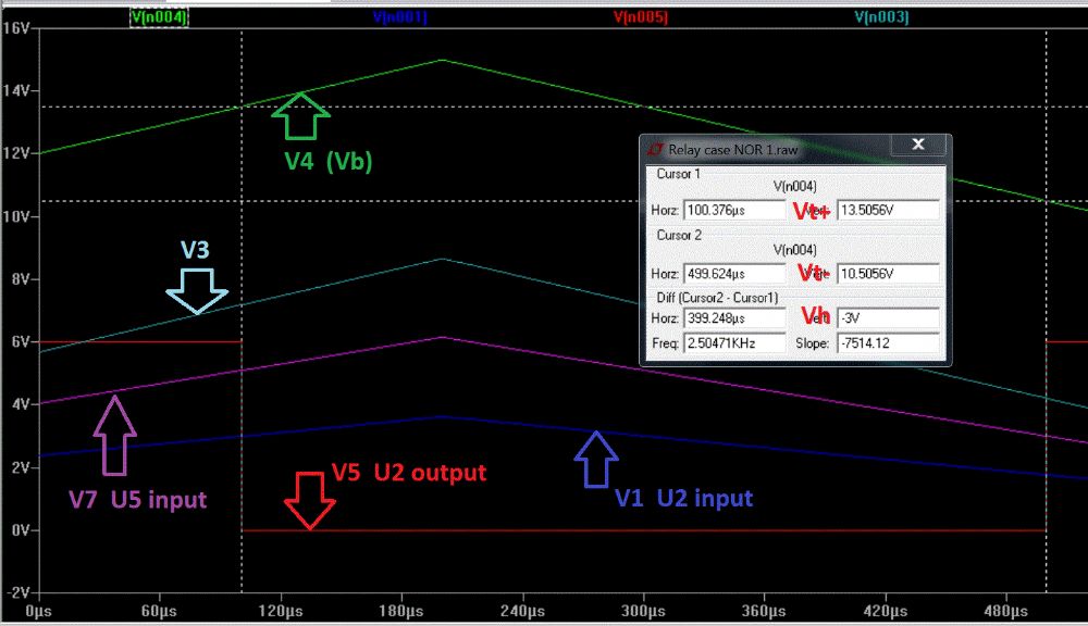
Jasper, Here is the NOR gate case & the .asc files. Len 2012-05-21_063945_Simulation_zip.zip 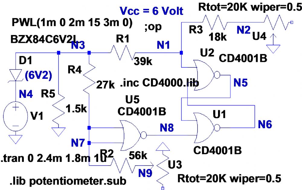
|
||||
| larny Guru Joined: 31/10/2011 Location: AustraliaPosts: 349 |
Tony, The only difficulty with the 555 (or 556) is that you can only alter the upper threshold. As you would know, the lower threshold is always Vu/2 so it varies with the upper one. Where Vu is the upper threshold. But that should not be a huge problem. Len |
||||
| SpmP Newbie Joined: 10/10/2010 Location: New ZealandPosts: 32 |
8) Cheers guys I will play with the spice and keep playing with the 358 solution. A real practical problem, not restricted to this design is that with half wave (and probably full wave) battery chargers, they are going to hit peak voltage well before the 'average' voltage is at our desired threshold. I guess this puts some onus on the battery charger to be somewhat descent, full wave with filter cap I guess... Jasper |
||||
| Warpspeed Guru Joined: 09/08/2007 Location: AustraliaPosts: 4406 |
Len, it does give very predictable switching points with known hysteresis. Any "tweaking" can be done by gain or level shifting ahead of the 555. Not a big issue, but it is both a simple and elegant solution. Cheers, �Tony. |
||||
| larny Guru Joined: 31/10/2011 Location: AustraliaPosts: 349 |
Cheers guys I will play with the spice and keep playing with the 358 solution. A real practical problem, not restricted to this design is that with half wave (and probably full wave) battery chargers, they are going to hit peak voltage well before the 'average' voltage is at our desired threshold. I guess this puts some onus on the battery charger to be somewhat descent, full wave with filter cap I guess... Jasper Jasper, There is another way to resolve this issue. You could insert a Low Pass Filter between the battery & the input to the Schmitt Trigger. There is also a way to eliminate your problems with Voh. I'm about to go out, so I'll post a suggestion later. Tony, I'll post my thoughts on the 555 solution later. Len |
||||
| SpmP Newbie Joined: 10/10/2010 Location: New ZealandPosts: 32 |
I have had the 358 solution running succesfully for a second day (shunt only), it seems alright, the waveforms are not amazingly clean, but acceptable, no blown fets today... Switching at 6-15kHz, and the heatsink sings like crazy! Tomorrow I will try 24V as the poor battery that has been sitting at 8V for far too long seems to have come back to life with some shunt (i.e pulse) charging 8) I had a go at the 555 circuit in LTSpice and managed to get both cases working. resistors on either side of the pots would help. Pot values are random. From the 555 datasheet it seems that Vth and Vtrig have upper limits, would zeners be sufficient to protect them? For some reason the wmf exports from LTSpice were not good enough, see the attached zip file. 2012-05-22_035633_555-Schmitt-trigger.zip Jasper |
||||
| larny Guru Joined: 31/10/2011 Location: AustraliaPosts: 349 |
Jasper, Here is how I would do the relay case using a 555. The Shunt case would be a variant - of course. I have assumed the use of a voltage doubler and a regulator to provide 15 volt for the 555. However, it could be configured to operate with a supply of 7.5 volt if you wish - but I don't recommend it as the low voltage complicates the issues - particularily for the Shunt Case. Adjustment procedure:- 1. Leave Vb open initially. 2. Set P2 to its maximum resistance. 3. Set the control voltage Vu to about 9.7 Volt. 4. Connect Vb to a 13.7 volt source. 5. Adjust P1 (reducing Vu) until the 555 output goes low. 6. Reduce the voltage at Vb to 10.4 volt (the 555 output should remain low) 7. Adjust P2 until the output goes high. Note that P1 should be adjusted first since it sets both the upper and lower thresholds inside the 555. I�ll post a low pass filter for you tomorrow. Len 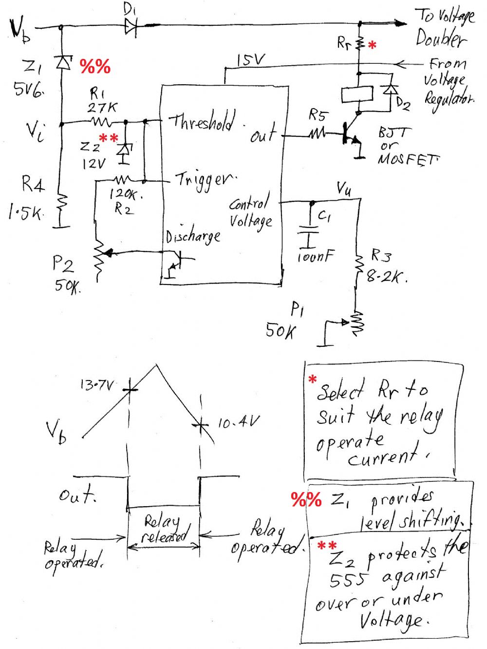
|
||||
| SpmP Newbie Joined: 10/10/2010 Location: New ZealandPosts: 32 |
Thanks Larny, Why would you not do it the way I have in the attached file? I tested the 358 circuit with 24V only modification was to add another same value resistor into the bottom leg of both voltage dividers. Worked perfectly. And again, considering that the 358 circuit is working, why should this not be implimented? Is it too loose (too many uncontrollable variables?). I guess the real test would be set and forget for weeks/years and is it reliable then? Jasper |
||||
| larny Guru Joined: 31/10/2011 Location: AustraliaPosts: 349 |
Why would you not do it the way I have in the attached file? Do you mean the 555-schmitt-trigger.zip file? I tested the 358 circuit with 24V only modification was to add another same value resistor into the bottom leg of both voltage dividers. Worked perfectly. And again, considering that the 358 circuit is working, why should this not be implimented? Is it too loose (too many uncontrollable variables?). I guess the real test would be set and forget for weeks/years and is it reliable then? Jasper Jasper, I'm providing you with options. The choice is yours. However, have you considered the temperature characteristics of the LM358 option? Particularily in the Shunt case, the hystersis is wafer thin so any changes due to temp or component aging will affect the performance. Another point to consider is that the reliability is an inverse function of the number of components. So the question is:- considering these issues, which option is the best? I can't answer that without spending a lot of time on it. I suggest you try cooling the PCB in a fridge, take it out & test it, Then heat it up with a hair dryer & test again. Compare these results with each other & with those measured at ambient temp. I'll post an active filter for you later. Len |
||||
| larny Guru Joined: 31/10/2011 Location: AustraliaPosts: 349 |
Jasper, The graph below is from the CMOS CD4049/4050 data sheet. It shows that the CMOS transfer function has virtually no variation with temp. This is the reason why I started (some days ago) to consider the CMOS options. The "threshold" is at approx Vcc/2 where the temp effect is close to or = 0. Len 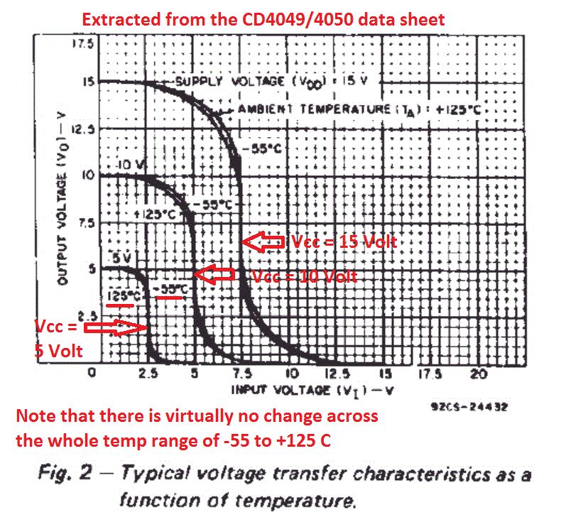
|
||||
| larny Guru Joined: 31/10/2011 Location: AustraliaPosts: 349 |
Jasper, I had another look at your circuit shown in 555-Schmitt-trigger_Shunt-Case.asc. It was a good idea to use a Zener diode as you did, however it suffers from three disadvantages:- 1. 3V3 Zener diodes have a significant temperature coefficient and abroad �knee�. 2. The pots attenuate the signal and thus reduce the hysteresis presented to the 555. However, it inspired me to think of a 555 solution that does not require attenuation of the signal and should have minimal thermal characteristics. So I�ll post the simulation tomorrow. Len |
||||
| larny Guru Joined: 31/10/2011 Location: AustraliaPosts: 349 |
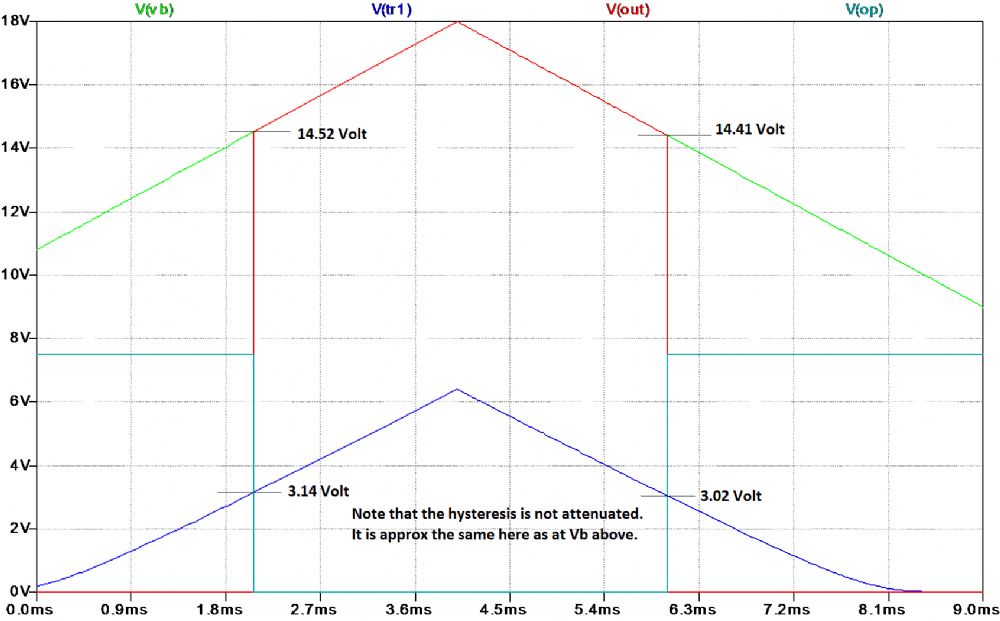
Jasper, Here is the simulation. Note that the hysteresis is not attenuated since the diodes have a very low dynamic resistance. You may be able to drive the MOSFET from the output of U4 via a resistor. If not, then you'll need a totem pole circuit. Diodes D1 & D2 should be replaced with two 5V6 Zeners since 5V6 have the lowest thermal coefficient. (I have not yet had time to load the 5V1 & 5V6 models into LTSpice.) I have not added any over voltage protection - that can be added later. I'll consider the relay case tomorrow. Len 2012-05-25_032437_Info.zip 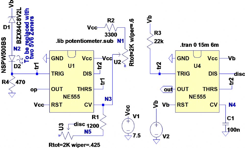
|
||||
| larny Guru Joined: 31/10/2011 Location: AustraliaPosts: 349 |
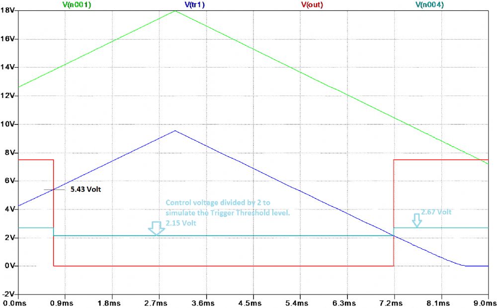
Jasper, Here is the relay Case. It is simpler & works a little differently to the Shunt case since it has a much bigger hysteresis. Len 2012-05-26_030342_Info.zip 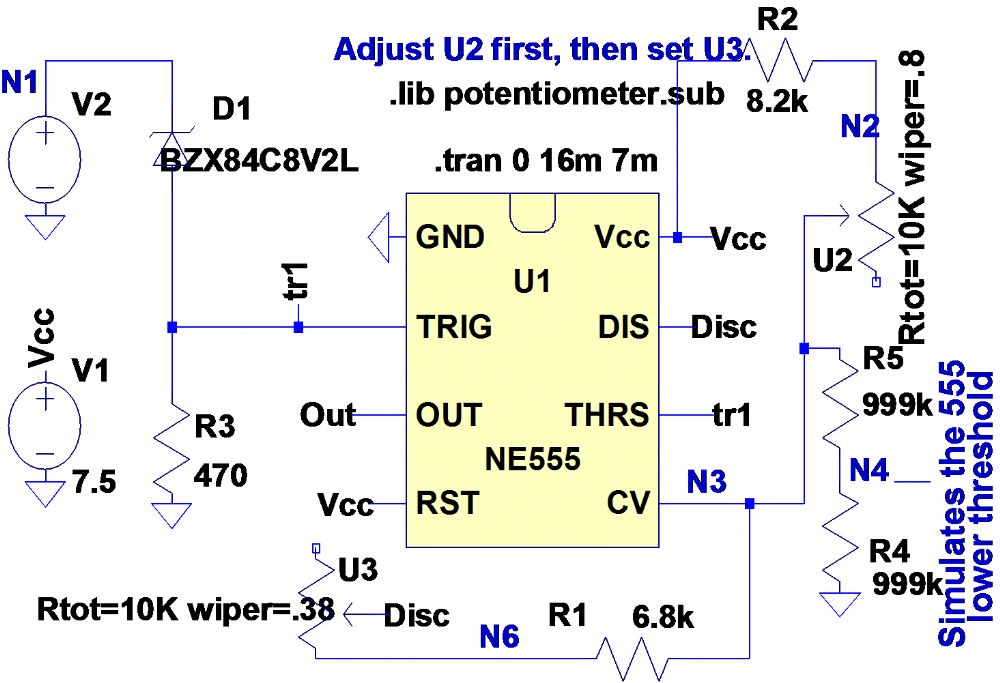
|
||||
| SpmP Newbie Joined: 10/10/2010 Location: New ZealandPosts: 32 |
Thanks once again Len, I a doing the pcb art etc. for the 358 soln. so I can put it in an oven/freezer etc., then will begin with the 555 and nor/nand solutions. Indeed options are a good thing, I guess the #1 design crime is sticking to your first idea 8), damn guilty, as charged. Jasper |
||||
| larny Guru Joined: 31/10/2011 Location: AustraliaPosts: 349 |
I a doing the pcb art etc. for the 358 soln. so I can put it in an oven/freezer etc., then will begin with the 555 and nor/nand solutions. Indeed options are a good thing, I guess the #1 design crime is sticking to your first idea 8), damn guilty, as charged. Jasper Jasper, You're welcome. I use prototyping PCBs rather than making up specials just for testing. The ones I use are sold by Jaycar, see www.jaycar.com.au and search for HP-9556 and HP-9558. Their photos are poor, so I have attached one that I took below. I have been thinking further about the CMOS solutions and will post somthing in a day or two. Len 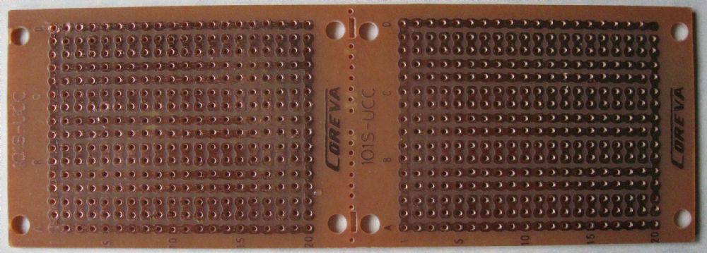
|
||||
| larny Guru Joined: 31/10/2011 Location: AustraliaPosts: 349 |
Jasper, Here is the JayCar prototyping PCB. I like this one since there are 3 holes in the horizontal strips. This better since you often need a 3 way connection. Len 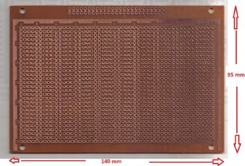
|
||||
| larny Guru Joined: 31/10/2011 Location: AustraliaPosts: 349 |
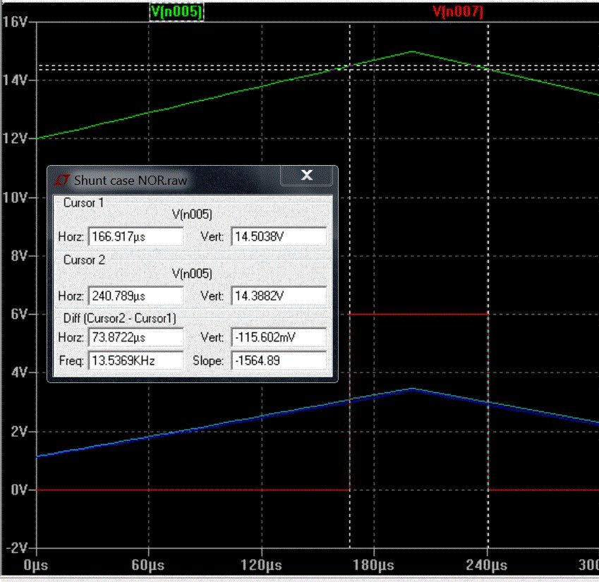
Jasper, Here are the CMOS options for the shunt case and the relay case. I have made some minor changes to the relay case that I posted some days ago. If you prefer to use NAND gates in lieu of NOR gates, then all you need to do is move U5 to the input of U1. You will have one spare gate, so I suggest you use it as a buffer between the flip flop output and the MOSFET or transistor. Brief description of the Shunt case circuit. The NOR gates U1 and U2 are configured as a flip flop. If the voltage at N1 is >3 Volt approximately, then the flip flop is set, i.e. out is high (6 Volt) and out_ is low (0V) � provided that the voltage at N8 is >3 Volt. If the voltage at N8 is <3 Volt approximately, the flip flop is reset � provided that the voltage at N1 is also <3 Volt. Adjustment procedure:- Set the voltage at N5 (i.e. V1) to 14.4 volt. Adjust U3 and U4 until the voltages at N1 and N8 are about 2.7 volt. Check that the flip flop is in the reset state. Adjust U3 (i.e. increase the voltage at N8) until the voltage at N9 goes low. Increase V1 to 14.5 volt. Adjust U4 until out goes high. Reduce V1 & check that the flip flop resets as V1 passes through the 14.4 Volt level. Len 2012-05-30_052258_Info.zip 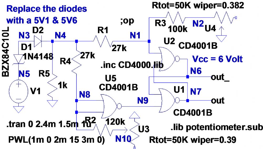

|
||||
| SpmP Newbie Joined: 10/10/2010 Location: New ZealandPosts: 32 |
OK, I havn't gone dead on this... I have made a pcb and been testing the opamp version. It snowed here in CHCH yesterday, and its bright and sunny today so I have got to test it in cold conditions, and will stick it in an oven this afternoon to see how the setpoint changes. BUT, I need advice here: First some pictures 8) 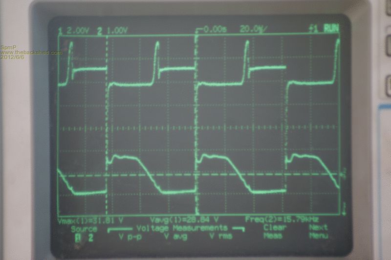
The upper trace is the voltage across the battery, sorry its a bit shakey, Vmax=31.81 Vav=28.84 F=15.78kHz, DeltaV~0.5V (I will change the hysteresis resistor to 660K and see what that does later on). Charge current 5.75A. The lower trace is Vgs for the FET. 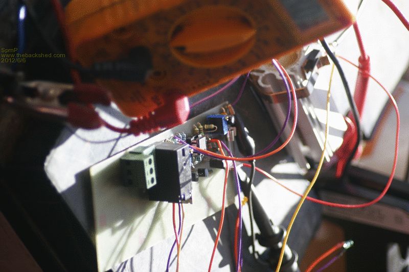
The circuit board etc. My dump load is 2x0.5m of nichrome wire in parallel (200W@28V) My problem is in evaluating the setpoint, whilst the FET is off, the voltage will jump to whatever the battery can hold it down to, and whilst the FET is on, drop to the battery and dump load in parallel. So... the problem, what do I measure as the setpoint? Vave, Vrms? Just use a cheap meter and hope for the best? As you can see on the scope trace there is significant over/under shoot on the edges. I assume they are roughly symmetrical when looking at Vave (they are not tho). And, I have a 33V zener acting sort of like a crowbar, but with the aim of blowing the fuse, under the assumption that if Vbatt > 33V the controller is malfuntioning, but... when the pannels are delivering full current in summer with ~9A I expect the battery voltage to spike higher than this. Does the zener need to be greater, the fuse a slow blow, or is my assumption way out. The other test to do is modify the mosftet drive circuit to be inverting such that the panels disconnect rather than the shunt load engages. I think this may be more appropriate for the ups/batteries in the cupboard rather than having 200W adding more heat 8) I suppose a better test of temperature dependence will be the 'relay case' with its wide hysteresis... --- Ok, next thing. Len, you have come up with a fantastic array of excellent circuits for this simple task. When I have finished understanding and playing with what I have here I will get on with the next option, but I wondered if you could outline some pro's and con's of the three different options. From my perspective I would probably want to try the nor/nand version next as it could be done with one package, whereas the 555 version will need either a 556 and a 555, two 556's or. three 555's. All are common. Unfortunatly the 558 has common CV etc. Anyway, thanks again! It sucks seeing all this energy being wasted as heat! But in summer this could be put to good use in an absorption fridge, where more sun=more cold, as it should be 8) (I was trying to do this directly at one stage with parabolic collectors and glycol... what a mess!) |
||||
| larny Guru Joined: 31/10/2011 Location: AustraliaPosts: 349 |
I havn't gone dead on this... I have made a pcb and been testing the opamp version. It snowed here in CHCH yesterday, and its bright and sunny today so I have got to test it in cold conditions, and will stick it in an oven this afternoon to see how the setpoint changes. BUT, I need advice here: First some pictures 8) The upper trace is the voltage across the battery, sorry its a bit shakey, Vmax=31.81 Vav=28.84 F=15.78kHz, DeltaV~0.5V What is DeltaV?(I will change the hysteresis resistor to 660K and see what that does later on). Charge current 5.75A.I could not see the time scale on the scope traces. The lower trace is Vgs for the FET. The circuit board etc. My dump load is 2x0.5m of nichrome wire in parallel (200W@28V) My problem is in evaluating the setpoint, whilst the FET is off, the voltage will jump to whatever the battery can hold it down to, and whilst the FET is on, drop to the battery and dump load in parallel. So... the problem, what do I measure as the setpoint? Vave, Vrms? It would help me if you posted your circuit. You have obviously changed it to work on 24 Volt. I don't really know how to answer the question. What is the purpose of the shunt? I presume it is to limit the voltage delivered to the battery. If so, then you would need to know what the battery limitations are. Just use a cheap meter and hope for the best? As you can see on the scope trace there is significant over/under shoot on the edges. I assume they are roughly symmetrical when looking at Vave (they are not tho). And, I have a 33V zener acting sort of like a crowbar, but with the aim of blowing the fuse, under the assumption that if Vbatt > 33V the controller is malfuntioning, but... when the pannels are delivering full current in summer with ~9A I expect the battery voltage to spike higher than this. Does the zener need to be greater, the fuse a slow blow, or is my assumption way out. I think you need a better solution. If you just blow the fuse, it will protect everything, but you loose the energy that would have been delivered to the battery & the load. The existing circuit is simply detecting the battery voltage. Perhaps you need a circuit that will detect the current also & thus switch in an extra shunt. The other test to do is modify the mosftet drive circuit to be inverting such that the panels disconnect rather than the shunt load engages. I think this may be more appropriate for the ups/batteries in the cupboard rather than having 200W adding more heat 8) I suppose a better test of temperature dependence will be the 'relay case' with its wide hysteresis...NO, I feel the Shunt case is better since the hystersis is so narrow hence any parameter changes due to Temp will be more noticable & potentially more critical. --- Ok, next thing. Len, you have come up with a fantastic array of excellent circuits for this simple task. When I have finished understanding and playing with what I have here I will get on with the next option, but I wondered if you could outline some pro's and con's of the three different options. From my perspective I would probably want to try the nor/nand version next as it could be done with one package, whereas the 555 version will need either a 556 and a 555, two 556's or. three 555's. All are common. Unfortunatly the 558 has common CV etc. Anyway, thanks again! It sucks seeing all this energy being wasted as heat! But in summer this could be put to good use in an absorption fridge, where more sun=more cold, as it should be 8)That would be a good idea.(I was trying to do this directly at one stage with parabolic collectors and glycol... what a mess!) I have to go out shortly, so I'll address the pros & cons in a later post. In the meantime, please post the circuit - I assume it is adapted by some means - for 24 Volt. |
||||
| larny Guru Joined: 31/10/2011 Location: AustraliaPosts: 349 |
I'm wondering about the spikes in the upper scope trace, did you adjust your scope probes for minimal overshoot/undershoot? As for the pros and cons of each circuit:- 1. The Op Amp one:- - It can be made to operate over a wide voltage range, ie. up to about 30 volt. - But it's switching is relatively slow. - Also the offset and output levels vary with temperature. - It may need more parts than the other options. 2. The CMOS version:- - Has the advantage that the transition level (as shown in the datasheet - see the extract that I showed in a previous post) has virtually no change with temperature. - The only disadvantage I can think of, is that the supply voltage is limited to either 15 Volt or 18 Volt, depending on which one you choose. So I suggest you download the data sheets of each version that you can find or buy. 3. The 555 option;- - Has some variation with temperature. - From memory, they have a maximum supply voltage of 18 volt. So I think you are right in testing the CMOS version next. |
||||
| The Back Shed's forum code is written, and hosted, in Australia. | © JAQ Software 2026 |