|

|
Forum Index : Microcontroller and PC projects : Ready to run PicoMiteVGA for GBP25 - good price?
| Author | Message | ||||
| Mixtel90 Guru Joined: 05/10/2019 Location: United KingdomPosts: 8781 |
VREG_VOUT on the RP2040 is the output of an on-chip 1V1 100mA regulator. The input to it comes from the 3V3 supply. It should have no direct connection to 3V3 as it powers the internal core! Mick Zilog Inside! nascom.info for Nascom & Gemini Preliminary MMBasic docs & my PCB designs |
||||
| JohnS Guru Joined: 18/11/2011 Location: United KingdomPosts: 4304 |
Ah, well 2R5 from there to 3V3 (however it happens) may be why things are very unhappy. I guess that's why the middle leg of the regulator is not much above 1V1. No worries, the other boards seem fine. And still great value. John |
||||
| Mixtel90 Guru Joined: 05/10/2019 Location: United KingdomPosts: 8781 |
The main regulator will be low because it's being pulled down by a heavy load. Most linear regulators have an internal reference voltage of about 1V25, so that's the lowest voltage that they will put out. It'll be current limiting to prevent it from cooking. If you have a very low resistance between VCC and GND then It will be very difficult to find without a surface mount rework setup as components will probably need to be removed until the fault clears. Far easier to let JLCPCB sort it out. :) Mick Zilog Inside! nascom.info for Nascom & Gemini Preliminary MMBasic docs & my PCB designs |
||||
| JohnS Guru Joined: 18/11/2011 Location: United KingdomPosts: 4304 |
Yeah, I suppose so, thanks. John |
||||
Quazee137 Guru Joined: 07/08/2016 Location: United StatesPosts: 603 |
John don't junk it. What the post from there to US? May be one of the local chaps would like it play with it? Quazee137 |
||||
| JohnS Guru Joined: 18/11/2011 Location: United KingdomPosts: 4304 |
Turns out the eprj is indeed enough - if you avoid the online EasyEDA and instead download & run the PC-based one (probably need the Pro version). For Linux users: after unzipping you also MUST make the easyeda-pro file executable! (FFS why isn't it already???) and of course then run it. There appears to be no README or INSTALL which if they existed would presumably point out the above. (It's quite a big download if all you really wanted was, say, the schematic PDF. Also, you have to get an activation code & input it.) It's all free AFAIK. John |
||||
| Mixtel90 Guru Joined: 05/10/2019 Location: United KingdomPosts: 8781 |
It had better be free - I've been using it for most of today. :) Still playing with a power supply design. Up to the 5th version on EasyEDA at the moment. I think this one is nice, but I've not done the control board. It's just the power handling one. I don't think it's me - some (not all) of the Phoenix PCB screw terminals appear to have their 3D models back to front! Mick Zilog Inside! nascom.info for Nascom & Gemini Preliminary MMBasic docs & my PCB designs |
||||
| George H Newbie Joined: 03/07/2020 Location: United StatesPosts: 33 |
Got my boards back and they all run fine as far as I can tell. |
||||
| Calli Regular Member Joined: 20/10/2021 Location: GermanyPosts: 74 |
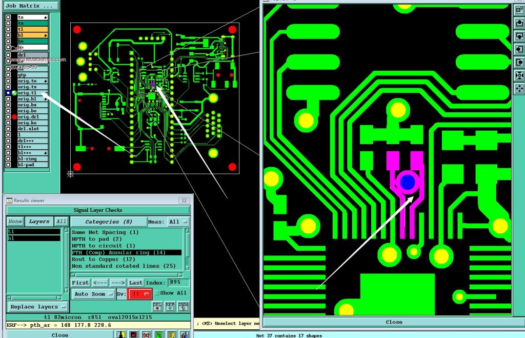
EDIT: I finally managed to open the .eprj file and checked that tey are indeed connected (VCC). Original: I tried and got this back:  Did I something wrong or are these meant to be connected? Best, Carsten Edited 2023-05-30 21:53 by Calli |
||||
| Mixtel90 Guru Joined: 05/10/2019 Location: United KingdomPosts: 8781 |
All three are connected on the VCC net. They are on my copy of EasyEDA anyway. :) Pins 48 & 49 are connected on the schematic. Edited 2023-05-30 22:19 by Mixtel90 Mick Zilog Inside! nascom.info for Nascom & Gemini Preliminary MMBasic docs & my PCB designs |
||||
| Calli Regular Member Joined: 20/10/2021 Location: GermanyPosts: 74 |
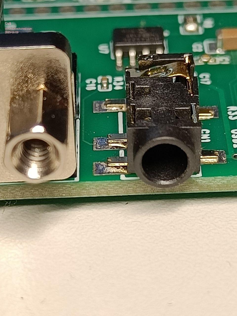
Hey hey hey! The boards arrived today. I could test 3 out of 5 for now and all work. The audio jack is however on all boards with raised legs soldered, I mean the small amount of solder paste couldn't connect the leg with the pad. Sometimes two and sometimes three legs, resulting in mono or no sound. Reflowed it with an iron and some flux and it works. Will mention JLBPCB about it. There is one thing to mention (did not search here thoroughly): OPTION AUDIO SPI GP24,GP22,GP23 lead to the Error that GP24 (and GP23) is already in use. I "solved" it with setpin gp24,off setpin gp23,off OPTION AUDIO SPI GP24,GP22,GP23 Not sure why that is. Incredible board, much fun! Best, Carsten |
||||
| Mixtel90 Guru Joined: 05/10/2019 Location: United KingdomPosts: 8781 |
I don't know if that's the usual audio jack, but the one used since the CMM2 has had two little locating pegs on the bottom to fit through holes in the PCB. I wonder if the jack was aligned properly or if the holes were too small? Either would cause the jack to be too high. Mick Zilog Inside! nascom.info for Nascom & Gemini Preliminary MMBasic docs & my PCB designs |
||||
| Calli Regular Member Joined: 20/10/2021 Location: GermanyPosts: 74 |
The jack used on my boards is complete SMT, I see no alignment pegs (EDIT: used a torch, there are pegs (very small ones) and they are all in the holes, not the cause). The placement is fine (maybe on some a bit rotated) and all legs hit the pads in sufficient manner, it is just that they are bent a bit up and there is not enough solder. I will try to get better images. But I think you can see that the solder does not connect. EDIT2: Maybe if the pads could be a bit smaller, so the body of the jack could settle better on the PCB, maybe it just floated a bit in the solder(paste)?  Maybe one can get different jacks and this is a worth a note for somebody who can't solder. Carsten Edited 2023-06-09 01:20 by Calli |
||||
| Mixtel90 Guru Joined: 05/10/2019 Location: United KingdomPosts: 8781 |
Interesting... Easy enough to reflow but you wouldn't expect them to come out like that. I suppose it might be tolerances on the jack or the lugs on it aren't fully clean so the flux & solder isn't flowing properly - especially if they are using lead-free or the flux is some sort of no-clean one and isn't aggressive enough. Edited 2023-06-09 01:32 by Mixtel90 Mick Zilog Inside! nascom.info for Nascom & Gemini Preliminary MMBasic docs & my PCB designs |
||||
| Calli Regular Member Joined: 20/10/2021 Location: GermanyPosts: 74 |
So I found a board (4 working) which will not upload the FW. It pops open the explorer window and you can throw in the FW. It seems that the transfer is quite a bit faster than normal. Board resets and the bing-beep it again shows the explorer window. Boot-switch is ok. Will grab schematics now and try to find something. Hints welcome. Best, Carsten |
||||
| Mixtel90 Guru Joined: 05/10/2019 Location: United KingdomPosts: 8781 |
I'd first look round the QSPI to the flash chip. It makes me think that the pico is loading the firmware but it's not getting written to flash. Mick Zilog Inside! nascom.info for Nascom & Gemini Preliminary MMBasic docs & my PCB designs |
||||
| Calli Regular Member Joined: 20/10/2021 Location: GermanyPosts: 74 |
Yep, will do! Thanks I will now document my journey. * I found that R23 is 1k instead of 10k and R4 is 1k instead of 10k. However I suspect the silkscreen is wrong here? Because at least one functional board has that too :) * I need a pause. And more pointy probes :) (and a bino, organizing one now) Edited 2023-06-09 22:59 by Calli |
||||
| Mixtel90 Guru Joined: 05/10/2019 Location: United KingdomPosts: 8781 |
The silk screen (on V1.1 anyway) is correct. With those two resistors reversed it's quite possible that it won't work. R23 (10k) is a pullup on the flash chip. The BOOT button puns that pin low via R4 (1k). If they are reversed then the pin probably isn't going low enough. Boards where it is working are probably only just managing it. Mick Zilog Inside! nascom.info for Nascom & Gemini Preliminary MMBasic docs & my PCB designs |
||||
| matherp Guru Joined: 11/12/2012 Location: United KingdomPosts: 11251 |
Just checked and the labelling is wrong on both versions. The little one is R23 10K and the one nearest GP0 is R4 1K Edited 2023-06-09 23:47 by matherp |
||||
| Calli Regular Member Joined: 20/10/2021 Location: GermanyPosts: 74 |
Ok, so I was right. (I mean it is obvious from the schematics, but I am a bit rusted reading and debugging things). I continue. C! |
||||
| The Back Shed's forum code is written, and hosted, in Australia. | © JAQ Software 2026 |