|

|
Forum Index : PCB Manufacturing : How to build a PCB design using Autotrax
| Author | Message | ||||
bigmik Guru Joined: 20/06/2011 Location: AustraliaPosts: 2980 |
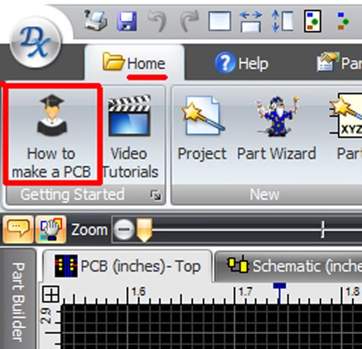
Hi All, Have you had a close look at the AutoTRAX DEX Home Page yet?? 
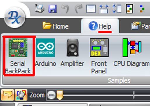
Or a look at the HELP page?? 
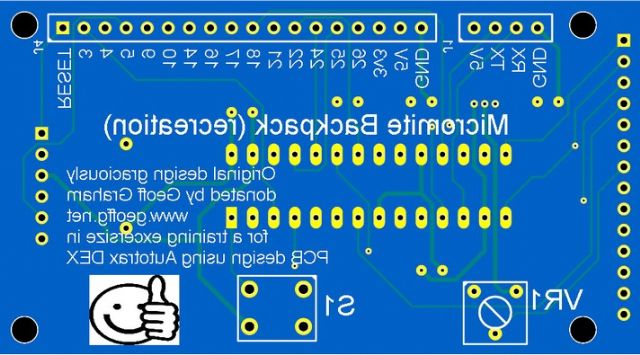
Yes, That is my `How to Build a PCB design Using AutoTRAX DEX' manual reformatted to suit a web page. AND My Serial BackPack (about to be replaced with a Ver 2) that I have allowed Iliya to add to DEX as an example. I guess I must be doing something right.. (well sometimes I might) Kind Regards, Mick Mick's uMite Stuff can be found >>> HERE (Kindly hosted by Dontronics) <<< |
||||
| yahoo2 Guru Joined: 05/04/2011 Location: AustraliaPosts: 1166 |
Hi Mik I have a question I cant seem to recreate a screenshot in the silkscreen section of the tutorial it is the bottom silkscreen viewed from the top with "pcb filled" checked in the layers menu, as soon as I do that the "current on top" box is greyed out. 
I cant decide if it is some transparency setting I have missed or a difference in newer software. I dont think it matters, I can view it with the "pcb filled" checkbox unticked or I can flip the board over and look at the bottom with the "view from" button. It's just been bugging me that i cant work it out  I'm confused, no wait... maybe I'm not... |
||||
bigmik Guru Joined: 20/06/2011 Location: AustraliaPosts: 2980 |
Hi Yahoo2, I just tried it and can confirm the same issue as yourself.. Iliya has either changed the way this works (layers UNDER the filled PCB) or it is some minor bug.. I will contact him and will let you know what he says. Kind Regards, Mick Mick's uMite Stuff can be found >>> HERE (Kindly hosted by Dontronics) <<< |
||||
bigmik Guru Joined: 20/06/2011 Location: AustraliaPosts: 2980 |
Hi All, As KOV.COM has changed its name to DEXPCB.COM the above link no longer works, The correct link is HERE!!! Regards, Mick Mick's uMite Stuff can be found >>> HERE (Kindly hosted by Dontronics) <<< |
||||
| mikedownunder Newbie Joined: 03/03/2016 Location: AustraliaPosts: 26 |
Hi Mick and others I have spent all of my hard earned cash this week purchasing the DEX software  . Really can't beleive the price for such a well designed piece of kit. . Really can't beleive the price for such a well designed piece of kit.I have been using Protel 99se vitually since its' inception way back when. So I was a bit daunted when I first started it, but thanks to Mick's tutorial  I pretty well soon got the hang of it. I pretty well soon got the hang of it. I finished the tutorial last night (Very late)   . . I like to make my own PCB's at home, (Love to get hands on and dirty)  . .I use the 'photographic' system where you use transparent paper and do a 1 to 1 on a UV sensitive PCB and was wondering whether Mick would like to add this to his tutorial. I figured that if I just leave the layer that I require, turned on in DEX, then I can print only that layer, which is ideal. However the first printout I did covered a whole A4 page and was not scaled to 1 to 1. I noticed in the Print Preview window of DEX there is an icon that says scale which was set to 100, I unchecked Auto-fit and after a bit of testing a 0 was the right scale. Not sure why, I thought it was a percentage, but maybe not. Anyway I have managed to print to the right scale and did each layer. My only problem is with the location of the print on the paper which is smack bang in the centre. This would result in a lot of wasted transparent paper. Protel has a system whereby you can place the image with a X Y cordinate, so it can be placed anywhere on the paper. Is there any way to contact Illyia and request this? Again thanks for a great tutorial. Mike |
||||
bigmik Guru Joined: 20/06/2011 Location: AustraliaPosts: 2980 |
Hi Mike, I am glad the tutorial was of some use to you.. I too came from Protel 99se to DEX. I bought DEX because it looked like Protel, but it did not work like Protel.. I had to forget all I had in my head and start again.. I wish a tutorial like I wrote was out there when I started.. I fought with DEX trying to get it to do things the way my mind thought (at the time) eventually I allowed DEX to do things the way it wanted and life was much easier.. As to adding the PCB link to the tutorial, I think the tutorial as it stands bar corrections is all I will put in it at this stage.. However if you want to write a tutorial on how to use DEX to print your artwork and then use that to generate a board I am sure many people would love to see that document. I am sure that Glen would allow it to be placed on The Back shed DocRegister. Regards, Mick PS. As to a way to contact Iliya you can do so through the DEXPCB Forum.. You need an invite code to access it but if you send me a PM with an email address I will send you an access code for the forum. Forum is at DEXPCB Forum Mik Mick's uMite Stuff can be found >>> HERE (Kindly hosted by Dontronics) <<< |
||||
TassyJim Guru Joined: 07/08/2011 Location: AustraliaPosts: 6512 |
Under the Help menu there is a 'wish list' option where you can submit a request. You can also use the forum for that sort of thing. Using the forum givers others a chance to offer alternative methods to achieve what you want. I use a CNC so don't have your problem and the issues I do have, I was ably to come up with a small program to edit the output to suit my requirements. I assume that you are printing using the PLOT option. I did a test and a scale of 'one' works for me. Try this: prepare your 'plot' Make sure your paper size is correct. Select an area on the plot view by dragging - it will automatically select the full page. Right click and 'copy' Open paint and 'paste' creating a full page image. select the region with the PC board and crop Print and adjust printing preferences (in paint) to 100% If you want to move the image to a spot on the page , when you select before cropping) select a larger area with blank space above and to the left to shift the printout. I did this on Windows 10 and it seems to work. Jim VK7JH MMedit |
||||
TassyJim Guru Joined: 07/08/2011 Location: AustraliaPosts: 6512 |
2016-09-29_051812_Printing_where_you_want_to_on_the_page.pdf Lucky it's a rainy day in Tassie I hope it is clear enough. Getting an option in DEX will be better. Jim VK7JH MMedit |
||||
| Paul_L Guru Joined: 03/03/2016 Location: United StatesPosts: 769 |
Is it possible to exchange PCB designs between AutoTRAK DEX and Sprint Layout 6? Does AutoTRAK DEX reliably import Gerber files written by other software? Is Sprint Layout 6 reliable when it imports Gerber files written by DEX? Sprint Layout 6 has a free viewer which lets you view any or all layers in a PCB design. Does AutoTRAK DEX have anything similar? Paul in NY |
||||
| The Back Shed's forum code is written, and hosted, in Australia. | © JAQ Software 2026 |