
|

|
Forum Index : Electronics : Wiseguy New Inverter Build Nano R6
| Author | Message | ||||
| bret76 Newbie Joined: 03/02/2023 Location: FrancePosts: 18 |
These diodes seems to be in parallel with the MOFSETS (red rectangles - D9..D16)? I don't see them on the BOM or on schematic, is this an option/outdated? 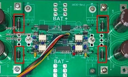 |
||||
| KeepIS Guru Joined: 13/10/2014 Location: AustraliaPosts: 2123 |
Hi, that is the Version 1 Power board, the Version 2 power board does not have them. The internal diodes in the HY5608 FET have a very high rating and these external "extra protection" diodes are no longer necessary. BTW we also stopped fitting them on the V1 boards. _ Edited 2024-09-09 08:03 by KeepIS NANO:Inverter V 8.2ks - Linux AvrDude GUI script V4.1 |
||||
| bret76 Newbie Joined: 03/02/2023 Location: FrancePosts: 18 |
Looking at the PCBs, I was wondering what is the use of the 2 red regions on the power PCB. At first, I thought that only the purple areas were useful, and that the red areas could be removed (easier access to the FETS, cheaper PCB), but it seems that you calculated these areas to limit the heating of the PCB. I was also wondering why the 120A connectors were in the middle of the PCB (at first glance, I would have put them on one side), but it is probably to distribute the voltage drop on each FET! 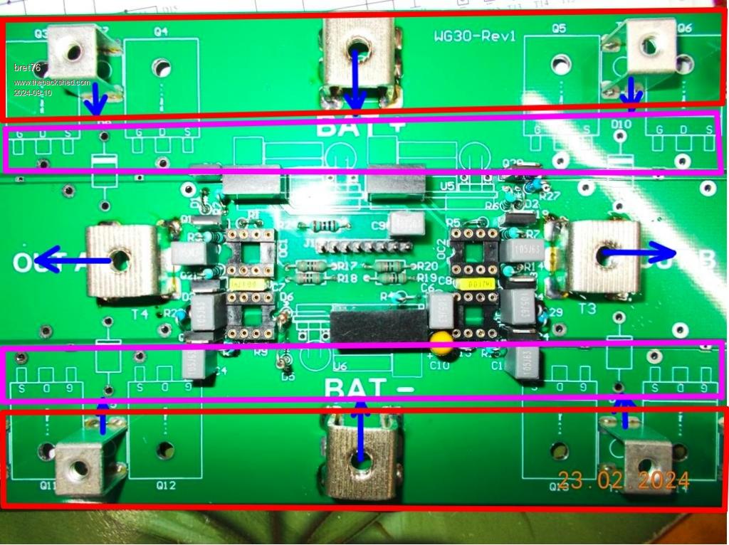 David |
||||
| bret76 Newbie Joined: 03/02/2023 Location: FrancePosts: 18 |
there are beads on the legs of the MOFSETS (L1 between A & B). As I understand it, it is a small inductance. When the MOFSET turns on, it reduces the current rise. Ok, I understand more or less. However, what happens when the MOFSET turns off? Can the inductance create a surge voltage that would destroy the MOFSET? Surprisingly, tests show that the MOFSETs resist (Brake down voltage = 80v). I am not sure of the numbers, nor of my calculation: bead = 0.26µH (poida tests) / Current 120A on 4 FET so 30A (guess value) / fall time 150ns (?) So: U=L x dI / dt = 0.26 * 30 / 0.15 = 52V Maybe there is saturation of the beads? If the battery voltage (lets say 56V) is share between upper and lower FET, each one "see" an additional 28V. For a rough calculation (52V+28V=80V) , it seem close of the limits no ? what am i missing? David 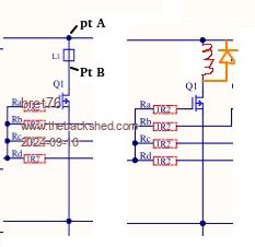 Edited 2024-09-10 05:44 by bret76 |
||||
| wiseguy Guru Joined: 21/06/2018 Location: AustraliaPosts: 1277 |
The width of the main + & - current carrying copper areas are both ~ 34.6mm. The 2 choke output copper area nodes are ~ 35.8mm, All the current carrying traces on the solder side of the PCB are the same as the areas on the component side so a total of ~ 70mm width of 2oz copper. Using a trace width/current calculator tells me that for a 15degC temperature rise, each side of the PCB will easily carry ~ 60A or a total of 120A which for ~50V supply is ~ 6KW. On either side of the PCB are two half bridges each consisting of 4 upper and 4 lower FETs, the whole PCB makes up 1 x full bridge consisting of 16 FETs in total for the 2 half bridges. By putting the + & - main 120A connectors at the PCBs centre, the current to each of the half bridge sides travels the shortest distance. Putting the + & - connectors on one end would cause greater overall voltage drop loss and a bit more heat. This is because as the inverter is running, the lower FETs on each side are turned on alternately each 180 degrees. Whilst one lower side is held on, the opposing lower side is busy with the SPWM switching. So there is current flowing on each side of the 120A "-" connector, whilst for the upper FETs current only flows on either side of the "+" connector alternately for each 180 degrees. The choke outputs ideally would be at the centre of each 35.8mm copper area of the middle traces, instead of one end closer to the PCBs centre (where they are). But to allow the use of the 2 x separate screw on capacitor PCBs this was not possible. I also had to make a notch out on the capacitor PCBs to allow space for the connector lug to the main PCB bridge outputs. If at first you dont succeed, I suggest you avoid sky diving.... Cheers Mike |
||||
| wiseguy Guru Joined: 21/06/2018 Location: AustraliaPosts: 1277 |
You are missing the link where I described the beads and the issues you mentioned. the link is Here In the end, I never bothered to put the resistors across the beads on the Power boards. The fact that a 15 ohm resistor "tamed" the spike with minimal heating in use showed the energy stored on the bead (yes it would be well and truly saturated) is in the tens of milliwatt region so I left them out. Avalanching of a FET is not harmful as long as the rated maximum is not exceeded, below is from the data sheet. EAS......Avalanche Energy......Single Pulsed......L=0.5mH......2829mJ The energy of the bead is a small fraction of the maximum avalanche energy, even at a 20kHz rate. The function of the bead is best considered as a high impedance to high frequencies component. Yes it is an inductor but its energy storage is really a small byproduct of its application here and can be be essentially ignored. From memory the bead was a 600 Ohm impedance at 100MHz but still had around 100R impedance at ~ 20MHz. The higher impedance on the Drain stopped the spurious oscillations from occurring. I don't think this is the best way to look at it, the battery voltage is not shared between upper and lower FETs. The upper FET has either zero or 56V across it, the lower has either zero or 56V. They don't like sharing at all (otherwise called destructive shoot through) so any inductive spikes are added to the 56V making a total of 56V + the value of the bead voltage calculated as ~ 52V or a theoretical maximum of 108V, so if we assume that the FET avalanches at its 80V maximum (never happens, will be at least 5 or 10+ volts above this) then we are only dissipating the narrowing "spike" energy somewhere above 85V. Edited 2024-09-10 12:06 by wiseguy If at first you dont succeed, I suggest you avoid sky diving.... Cheers Mike |
||||
| KeepIS Guru Joined: 13/10/2014 Location: AustraliaPosts: 2123 |
Just a quick  for that New V2 power board. for that New V2 power board.I found it really nice to build compared to the V1, I built a V1 and V2 side by side the other day, I really appreciated the rearrangement and extra simplification, and of course the V2 worked first go, V1 needed a resistor removed where there should have been a link, I was tired and it was the last couple of resistors on the V1  _ Edited 2024-09-10 16:36 by KeepIS NANO:Inverter V 8.2ks - Linux AvrDude GUI script V4.1 |
||||
| wiseguy Guru Joined: 21/06/2018 Location: AustraliaPosts: 1277 |
I agree the Power PCB was a faster easier build, once the circuit had been proved and refined, all surplus (redundant) parts provisions were removed saving a lot of links and also simplifying the track layout. Thanks for your prompting about the input diode that was in series with the pre charge resistor and it too being redundant now. I am posting the latest schematic with the minor mods at the input (diode removed) including running the Kilovac from the bulk capacitor side of the precharge resistor instead of the 48V supply side, it makes almost no difference either way. 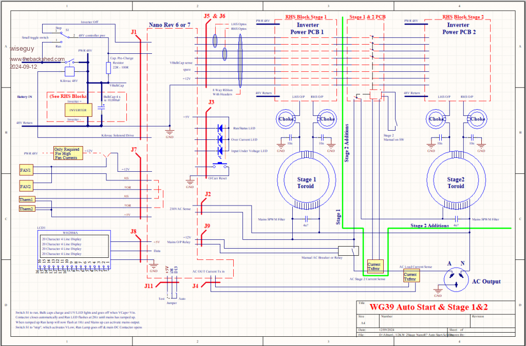 PDF for better resolution 12KW 2Stage NanoR7 Auto Start.pdf If at first you dont succeed, I suggest you avoid sky diving.... Cheers Mike |
||||
| Cpoc Senior Member Joined: 28/05/2024 Location: PortugalPosts: 109 |
Wiseguy whenever you believe the hardware is ready you can go ahead and order the PCB. Some more testing wont hurt. This new design is the perfect balance of power and energy savings. |
||||
| wiseguy Guru Joined: 21/06/2018 Location: AustraliaPosts: 1277 |
Ok been busy, I have raised the Rev of the WG30 power board to REV3. I know my use of the vertical resistors were keeping Klaus awake at night so I have sorted that. Due to the links diodes etc that were no longer required I massaged the spaces a bit and all diodes and resistors lay flat. This was initially impossible but with the parts minimisation voila a half day and its done. No parts changes but on the parts list where it says 0.2" spacing resistor (vertical) it should say 0.4" and laid flat, similarly for the 2 x zeners. 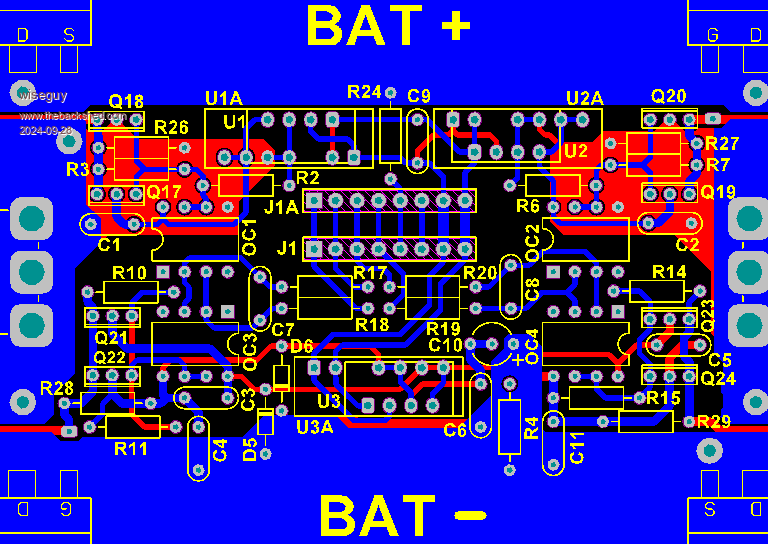 I also needed a simple panel for Vin/Vcap low LED, Run LED and over current LED and reset switch with labelling, so I turned to a PC solution, about 65 x 72mm. It fits Phoenix din rail PCB mount carrier also some cheapie look alikes from our good friends at Ali who never copy anything but are very inspired by others work  All the PC traces are on the rear of the PCB and I bought some long 6 pin ribbon with 0.1" spacing headers fitted (also Ali) to simply connect the panel and controller together. 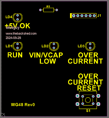 At this stage I am making my dual stage inverter a minimalist device for 2 reasons. I want the least number of indicators and switches I can get away with and so others would not feel intimidated to turn it on and interpret the lights etc. Besides I hate all the extra wiring and fitting of stuff - I think I am basically a bit lazy when it comes down to it. Thanks to KeepIS for his ground work - apparently it may never fail so all the extra monitoring stuff becomes redundant  I might still add another switch and LED (and connector) to the Panel for the second stage manual switch and LED if used, might as well mop up as much as I can. If at first you dont succeed, I suggest you avoid sky diving.... Cheers Mike |
||||
| KeepIS Guru Joined: 13/10/2014 Location: AustraliaPosts: 2123 |
Great refinement of the Inverter PCB, this will make the project even simpler for new builds. You are right, everything I've seen with all of the monitoring I have, indicates only minimal monitoring will be needed for this Dual inverter, BTW I like that indicator breakout and reset PCB addition. NANO:Inverter V 8.2ks - Linux AvrDude GUI script V4.1 |
||||
| wiseguy Guru Joined: 21/06/2018 Location: AustraliaPosts: 1277 |
Newbies Ric M, Bret76, Cpoc, JustinH, I have sent you all pms to confirm your requirements. Cpoc has replied to that. If you like or and want some of the front panel options (WG48) please let me know in your reply via PM. I can throw one in for testing no cost if you are not interested in more than 1. If at first you dont succeed, I suggest you avoid sky diving.... Cheers Mike |
||||
| Murphy's friend Guru Joined: 04/10/2019 Location: AustraliaPosts: 674 |
Ha, no chance to keep me awake at night with your PCB design   . .However, I might keep you awake with yet another PCB layout suggestion. I don't know how many boards you have ever repaired but I always curse the designer for placing too small a pad when there is lots of room for bigger ones. Big pads = less chance to lift them if a component needs to be unsoldered. For example, I always use rectangular pads with rounded corners for IC's. Pin 1 is marked on the silk screen, you can see that even after an IC socket is soldered in. I generally use square pads (instead of round) for components. Usually, only test pins have round pads for easy IDing on my boards. But I do appreciate you having used sensible size PCB tracks  . . |
||||
| bret76 Newbie Joined: 03/02/2023 Location: FrancePosts: 18 |
I will skip the actual M6/M4 expensives connectors and put a spacer. So I will drill the PCB, perhaps it will be more accurate if the factory drill it. Is it possible? I don't want to mess, so if not possible / to late / too complex / more expensive...don't bother. 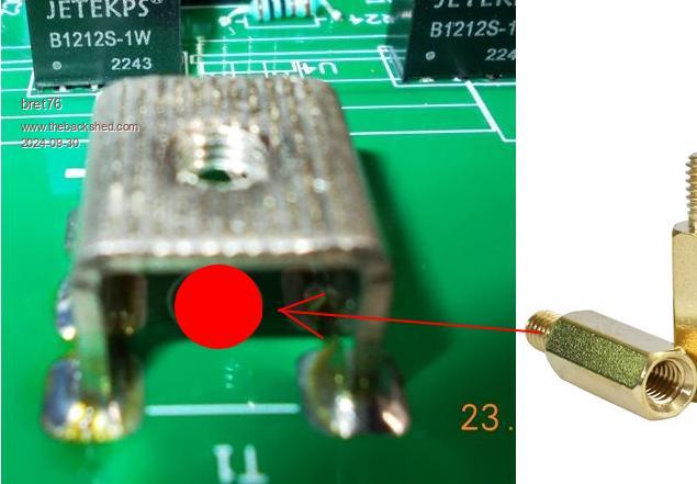 |
||||
| wiseguy Guru Joined: 21/06/2018 Location: AustraliaPosts: 1277 |
It would be helpful if you had hinted what size hole was desired for the spacers? Would you use the same spacers for the cap PCBs too ? A data sheet for the spacers or at least a part number or description of the spacers ie hex and the dimensions across the flats etc. I may have done something but instead I spend time answering your email in a bit of depth. What current/power levels are you expecting from your inverter? The spacers may not be adequate for the current for the main power connectors which are rated for 120A and distributed over 6 points and not concentrated on a single point like a spacer. Spacers should be ok for the cap boards but spending 7.4 euros total and using 4 PC7s per cap board (8 per inverter) would sort your 2 inverters with 4 spares left over ? I just checked online. The large terminals can be purchased through ALI in lots of 5 terminals & screws and free freight for ~ E7.8 euros https://www.aliexpress.com/item/1005006747470675.html The cap board terminals can be purchased in lots of 20 for ~ E7.4euros including freight. PC5 https://www.aliexpress.com/item/32811408567.htm Personally I would have thought that these prices are reasonable solutions without having to modify the PCBs further. I am not really keen to modify the power boards further now as it would delay the PCB orders further and I am a bit time poor at the moment. If at first you dont succeed, I suggest you avoid sky diving.... Cheers Mike |
||||
| bret76 Newbie Joined: 03/02/2023 Location: FrancePosts: 18 |
No problem, leave it like it is. David |
||||
| Cpoc Senior Member Joined: 28/05/2024 Location: PortugalPosts: 109 |
Thank You wiseguy for providing those links. I was trying to hunt those down at good prices. |
||||
| wiseguy Guru Joined: 21/06/2018 Location: AustraliaPosts: 1277 |
Boards order still not sent yet.  Have incorporated second stage manual switch LED & connector on to the front panel which now looks a bit better. When I went to get the link for the Din Rail PCB assembly there was nil stock now and I found it a bit problematic to find others so I hedged my bets and provided 3 ways to mount. 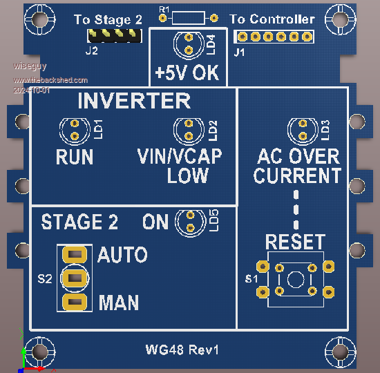 The item that mounts & encloses the PCB edges is out of stock: https://www.aliexpress.com/item/1005006602242361.html It is originally a Phoenix part and can be found in Farnell and Digikey there may be other suppliers and manufacturers but the Phoenix solution is a bit dear The board may have to have the "ears" for option 2 cut off to fit the enclosure the main board dimensions (less the ears) are 72mm H x 65.7mm W Option 2 https://www.aliexpress.com/item/1005007804893889.html Option 2 screws to the board either side and can then clip the unenclosed PCB to the din rail. There are 2 small PCB cutouts to allow the din rail to be unclipped with a small screwdriver. Option 3 is to use the 4 x 3mm mount holes at the corners of the board. The toggle switch allows the solder tag type connects to be inserted into the board it does not have to be the PCB pin type. I also added holes to suit 4mm spacers on the main power PCB for the cap boards and also at the centres under the main power connectors for Bret76 seeing as I am tidying up stuff and delayed anyway, the holes also allow for drilling larger holes accurately for bigger spacers bolts etc. Sample portion of power PCB mods below. 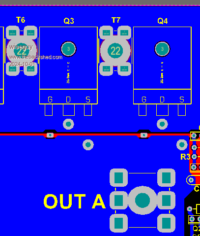 Edited 2024-10-01 12:27 by wiseguy If at first you dont succeed, I suggest you avoid sky diving.... Cheers Mike |
||||
| Cpoc Senior Member Joined: 28/05/2024 Location: PortugalPosts: 109 |
Nice  That is a slick design. |
||||
| bret76 Newbie Joined: 03/02/2023 Location: FrancePosts: 18 |
You study every point in detail  ! I am impressed. Well done and thank you. ! I am impressed. Well done and thank you.  |
||||
| The Back Shed's forum code is written, and hosted, in Australia. | © JAQ Software 2026 |