|

|
Forum Index : Electronics : Wiseguy New Inverter Build Nano R6
| Author | Message | ||||
Revlac Guru Joined: 31/12/2016 Location: AustraliaPosts: 1241 |
Mike, I'm totally happy with what I have, and should be no drama to do the fix,  I was thinking before, one of those dremel diamond cylinder bits might do it neatly, or anything better? I was thinking before, one of those dremel diamond cylinder bits might do it neatly, or anything better?Cheers Aaron Off The Grid |
||||
| wiseguy Guru Joined: 21/06/2018 Location: AustraliaPosts: 1277 |
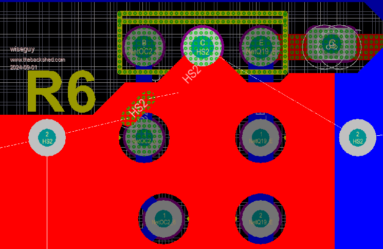
And now for a giant serve of humble pie. I had a niggling thought could I have made a mistake, no don't be silly! I made a mistake once it was a Tuesday - I thought it would rain but it only sprinkled  . .I decided to re-check the files that I sent to JLPCB and did a design rule check on them and was instantly rewarded with an error!! Crap it was me all along this time. I used a ground-plane to connect some points that were previously joined with a track. Then I deleted the track but a small segment obviously did not delete and caused the short. I have a rule to always run a DRC check no matter how small the change I make. Somehow I either did this but the track segment was moved when looking around/checking and I did not notice it or I forgot to do the DRC check. Here is a picture where you can see the offending track segment. Sorry - there will be no replacements coming you will have to do the surgery  At least I found it and owned up and apologised to them before they investigated it.  Edited 2024-09-01 12:10 by wiseguy If at first you dont succeed, I suggest you avoid sky diving.... Cheers Mike |
||||
Bryan1 Guru Joined: 22/02/2006 Location: AustraliaPosts: 1889 |
I checked mine just now and yes R6 was shorted so gave it a scrap but still shorted, measured the hole and found a 1.2mm drill bit so put that thru and with another light scrape problem fixed and the underside track to Q20 is still valid. Regards Bryan |
||||
| Cpoc Senior Member Joined: 28/05/2024 Location: PortugalPosts: 109 |
Wiseguy it was not your fault it was Agatha All Along. It was good of not only to admit to the error but show everyone else how to fix it. |
||||
| KeepIS Guru Joined: 13/10/2014 Location: AustraliaPosts: 2123 |
I guess as a last resort, it should be easy to just drill out the through hole and solder R6 between HS2 and base of Q20 or 6,7 of OC2 or some variation. Just a minor hiccup really  NANO:Inverter V 8.2ks - Linux AvrDude GUI script V4.1 |
||||
| phil99 Guru Joined: 11/02/2018 Location: AustraliaPosts: 3176 |
You don't need to drill all the way through, just that copper layer as you would do with stripboard tracks. A 1/8" drill (or perhaps a little bigger in this case) held in a Bluepoint connector and twist by hand. No risk of going too far then. |
||||
| mab1 Senior Member Joined: 10/02/2015 Location: United KingdomPosts: 280 |
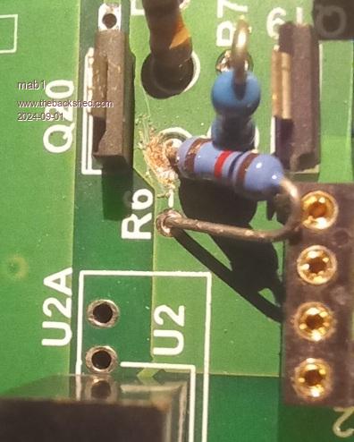
 not a problem. I used a soldering iron to raise R6 a mm without actually removing it, then bent it to one side. Tried my usual track cutting tool (end tooth on a junior hacksaw blade) but the pin through its end blocked that (Q20 too close), so just used the tip of a needle file. not a problem. I used a soldering iron to raise R6 a mm without actually removing it, then bent it to one side. Tried my usual track cutting tool (end tooth on a junior hacksaw blade) but the pin through its end blocked that (Q20 too close), so just used the tip of a needle file. Not pretty, but once R6 is back in position who's going to see it?  |
||||
| Murphy's friend Guru Joined: 04/10/2019 Location: AustraliaPosts: 674 |
Sorry about your "humble pie" episode. Yes, those fancy auto routing PCB layout programs can get you when you least expect it. I'm so glad I stuck to my old fashioned way to do PCB's, choosing my own pad & hole sizes. Not a fan of placing resistors vertically either, one has to be careful the long leg never gets bent over to touch something it shouldn't. |
||||
| wiseguy Guru Joined: 21/06/2018 Location: AustraliaPosts: 1277 |
This is a good time to review PCB design. I don't use any auto routing feature and haven't since 1986 after I decided they were next to useless and made awful messes of a quite straightforward task, they may be better today but I still won't trust them. The PCB layout program I use is not at fault, I accept responsibility for the mistake. I have no issues with the old fashioned ways thats how I started back in the late 70's but I don't have the time these days and have progressed to very efficient PCB design software. When currents exceeding 200A are being switched I do not believe in making larger PCBs just to lie resistors flat. I had three options one was to use surface mount resistors the other was to use vertical through hole parts the last was to use a vertical PCB. I chose vertical resistors and am very comfortable with the result. A lot of care was taken though to ensure with orientation and spacing it was next to impossible for resistor legs to touch anything adjacent. If anyone manages to get stuff touching they shouldn't complain about whatever the result is. Edited 2024-09-01 23:41 by wiseguy If at first you dont succeed, I suggest you avoid sky diving.... Cheers Mike |
||||
| Cpoc Senior Member Joined: 28/05/2024 Location: PortugalPosts: 109 |
Wiseguy don’t’ sweat it we all make mistakes but it takes a real man to admit to them. In my youth I did a lot of pcb rework jobs when I had perfect eyesight. You have no idea how many reworks had to be done because a pcb run had a small error in it and I was the guy to do it. It’s not a big deal. It was either scrap the whole pcb batch or do the rework. Back then pcb was not that cheap as it is today. |
||||
| bret76 Newbie Joined: 03/02/2023 Location: FrancePosts: 18 |
On the control board WG39-Rev7, the A7 output seems not used. Is it possible to connect it to a connector (Main up relay pin 2 or Sync Provision pin 2)? If it is not possible, i can sold a wire or use one of the LED output. I want smooth the load (use the maximum energy when sunny and keep battery for the night). The goal is to drive an SSR (ON/OFF) to increase / reduce the load of the water heater and perhaps electic car. Somethink like : oh the battery is nearly empty and power is >5kw : reduce load. Or : the battery is full, and I use only 500W : increase load and use as max energy as possible. Actually, when my battey is full, I need to reduce solar power.  Can I use the "O/Curr LED" or is this one reserved for a security function in the code? David |
||||
| wiseguy Guru Joined: 21/06/2018 Location: AustraliaPosts: 1277 |
The A7 analog input is grounded, with my hardware and Poida's software it removes offsets by reading A7 before reading AC current. KeepIS has created his own version of software which I understand he does not need/use the A7 read, so with his software I understand it would free up A7. The D2 Sync input is not implemented in Poidas code and as you are looking for an output, it would allow you to use this pin in his Code. I am unaware if KeepIS has utilised this pin for anything. I am already software challenged and to be honest I do not want to try to get my head around 2 lots of code, so as Poida was good enough to support my Inverter and Variac projects and write the code for them, I became quite familiar with it whilst debugging & testing. KeepIS has heavily changed the original code and it runs his Inverter well. My suggestion on how to proceed with the project would be to use my hardware and Poidas code as is for a starting point and I am able to provide support to get the inverter up and running. When you are happy with its performance then consider further how you would like to implement the battery monitoring functionality. As a suggestion, perhaps consider using an external circuit, using either analog (using a dual or quad comparator) or a separate Nano could provide the battery monitoring function to control external switching of loads depending on the battery SOC. Then a mistake in code would not harm the inverter ? The overcurrent LED is not driven by code it lights when the overcurrent latch Q1/Q2 is triggered (Q1 drives it on). Edited 2024-09-03 12:28 by wiseguy If at first you dont succeed, I suggest you avoid sky diving.... Cheers Mike |
||||
| KeepIS Guru Joined: 13/10/2014 Location: AustraliaPosts: 2123 |
FYI Found a quick neat method to remove the short on R6 on the top of the PCB that works for me. It took all of 3 seconds, I just used a small drill bit held between my fingers to remove the top through solder pad, it also removes the copper that projected into and shorted the top pad. IMHO it does not compromise the solder connection on the bottom of the PCB, and from my perspective the board is now 100% perfect. Anyone who has worked with Veroboard would be familiar this, twisting a small drill bit between you fingers to neatly cut the copper tracks. R6 solders in perfectly of course and no more short, the mod is virtually invisible, no scrape marks or slip marks. I've just started building two more power boards and was going to use two V1 boards, but I suddenly thought of this, tried it, and it was so simple and neat that I will be using this V2 board and one V1 board. EDIT: Reading back phil99 mentioned something similar, his mention of Bluepoint connector threw me and it didn't register.. _ Edited 2024-09-06 11:36 by KeepIS NANO:Inverter V 8.2ks - Linux AvrDude GUI script V4.1 |
||||
| phil99 Guru Joined: 11/02/2018 Location: AustraliaPosts: 3176 |
Holding the drill in a connector saves your fingers getting cut on the flutes when doing a lot of Vero cuts. |
||||
| KeepIS Guru Joined: 13/10/2014 Location: AustraliaPosts: 2123 |
I hold the drill shaft, long fingers   NANO:Inverter V 8.2ks - Linux AvrDude GUI script V4.1 |
||||
| Murphy's friend Guru Joined: 04/10/2019 Location: AustraliaPosts: 674 |
There is also a special tool available for that. It's just a bit with a nice plastic handle. That came in handy back when I did a lot more veroboards. Nowadays I prefer doing PCB's since they are so cheap. |
||||
| wiseguy Guru Joined: 21/06/2018 Location: AustraliaPosts: 1277 |
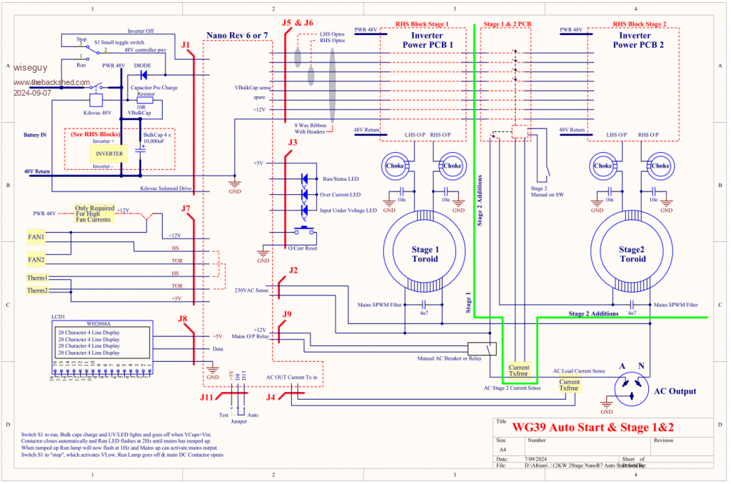
I am still busy building up my inverter and now I have got to the wiring up stage, it is the right time to properly draw up the overall schematic. So below is the schematic showing the first and second stage wiring overview. The division between a single stage inverter and the added parts for the second stage has been highlighted with the green dividing line between the two stages. Gee it looks simple enough to also add a third stage  In building up my 2 stage inverter, I have decided to start with the simplest implementation for it. I will not be providing for all the separate input DC peak hold & DC & AC overcurrent trips for each of the stage1 & stage2 that KeepIS has done. Time will tell if these are needed (I am hoping not). Maybe I might add just the one input DC current sensor for the main input current peak hold & over current trip circuitry already provided for on the stage 2 switching PCB. Not sure of the picture resolution so I have a PDF below it for best quality.  12KW 2Stage NanoR7 Auto Start.pdf Edited 2024-09-07 14:25 by wiseguy If at first you dont succeed, I suggest you avoid sky diving.... Cheers Mike |
||||
| KeepIS Guru Joined: 13/10/2014 Location: AustraliaPosts: 2123 |
Diagram looks nice, sure looks simple to add the 2nd or a 3rd stage  I agree that some of the extra monitoring may not be needed, and of course in time I'll at least get a good idea. I muse apologize for not testing the 2Stage circuit yet, I know it's going to work though. Instead, I spent yesterday afternoon and today building two new Power boards with all ferrite beads and the included late suggested changes, I just finished them now. I feel that a second AC over current sensor with a burden resistor and adjustment pot fed into the Ext input might still be a good idea though, otherwise the AC over-current value from the main AC feed will remain the same for both 1 or 2 stages powering the load. I guess it depends on how you are planning to set the one AC over-current value. Maybe limited to what a single stage could safely handle and trip at, and just use the second stage to share the load and keep things cool at higher power levels? _ NANO:Inverter V 8.2ks - Linux AvrDude GUI script V4.1 |
||||
| wiseguy Guru Joined: 21/06/2018 Location: AustraliaPosts: 1277 |
Yes I do agree, I was wondering if I could use the spare wire on the 8 way opto cable to feed back a signal from the second stage controller to reduce the sensitivity of the latch input using a small signal FET etc and thereby effectively doubling the current trip point, without upsetting the output current readback calibration. Still throwing around ideas but I am just wanting to get it running at this stage and tidy up the loose ends later. I will probably end up hacking that current sense circuitry corner from a new PCB and mount it on a spacer, not too unlike like what you did for the peak meter lol (I did notice). Edited 2024-09-07 18:53 by wiseguy If at first you dont succeed, I suggest you avoid sky diving.... Cheers Mike |
||||
| KeepIS Guru Joined: 13/10/2014 Location: AustraliaPosts: 2123 |
Yes a number of simple ways to do it. BTW I'll be swapping the two new power boards into the Inverter in the morning, hopefully everything goes to plan. NANO:Inverter V 8.2ks - Linux AvrDude GUI script V4.1 |
||||
| The Back Shed's forum code is written, and hosted, in Australia. | © JAQ Software 2026 |