
|

|
Forum Index : Electronics : Started Buck converter project
| Page 1 of 5 |
|||||
| Author | Message | ||||
| govertical Guru Joined: 11/12/2008 Location: United StatesPosts: 383 |
Hi, after watching a video on MPPT, I was inspired to fabricate a buck converter circuit to determine if it will improve turbine output and performance. The core of a MPPT is a micro controlled buck converter. I am starting with a basic circuit, just the buck converter using a fixed switching frequency. In theory the circuit should convert a high voltage low amp signal from the PMA to a lower voltage high amp signal to the battery bank. The circuit should negate the affects of the stators internal resistance and help prevent a stall condition at the turbine. The test circuit will have a 5 amp max output to start and if I can get the circuit functioning I will parallel the MOSFETs and diodes for a higher amp output. Comments welcome. 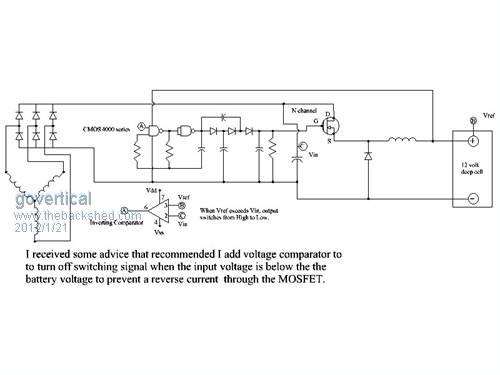
just because your a GURU or forum administer does not mean your always correct :) |
||||
| herbnz Senior Member Joined: 18/02/2007 Location: New ZealandPosts: 258 |
Hi your on the right track here. I have been working with thi idea for years but time constraints and facilities have prevented the building of a buck converter from scatch. I have used old PC supplies modified but laterly I have lashed out and bought a commercial solar MPPT (Tristar ) Using it on Hydro's and windmills it works brilliantly but cost and lack of being able to get in and alter the prog means I will watch your progress here with interest. Herb |
||||
| govertical Guru Joined: 11/12/2008 Location: United StatesPosts: 383 |
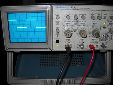
Hi, I am mainly interested in finding out if it will improve turbine performance by reducing the affect of the stator internal resistance. If it does than I can up grade the circuit. The new used oscilloscope arrived and I spent the few days trying to get the nand gate oscillator to oscillate and show the output wave form on the O-scope. Step one complete, next is the voltage multiplier. I will post updates when available. 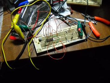
just because your a GURU or forum administer does not mean your always correct :) |
||||
| Warpspeed Guru Joined: 09/08/2007 Location: AustraliaPosts: 4406 |
Just looking at that circuit, I suspect you are going to have some problems with the MOSFET gate drive circuit. What is needed is a proper "high side" gate driver chip such as the top half of an IR2110 Cheers, �Tony. |
||||
| govertical Guru Joined: 11/12/2008 Location: United StatesPosts: 383 |
Hi, I used the same circuit for a bidirectional motor controller. I am just trying to get a basic circuit working so I can manually spin the PMA to determine if it helps remove the affects of the stators internal resistance. I am still doing research on gate driver IC�s. I am not recommending this circuit, I am piecing it together from unused items from other projects. I am sure there are better options. Thank you for the recommendation. So far I have the oscillator and voltage multiplier working, I should be able to add the comparator and mosfet soon. just because your a GURU or forum administer does not mean your always correct :) |
||||
| govertical Guru Joined: 11/12/2008 Location: United StatesPosts: 383 |
Hi, your observation is correct. The RC timing constant at the voltage multiplier output is not allowing a pulsed output. The output of the voltage multiplier has 1.5 volt ripple riding 20 volts and is not discharging to zero, so the MOSFET will never turn off when point A is enabled. I am searching for alternatives. Ordering a gate driver is the obvious solution. Comments welcome. 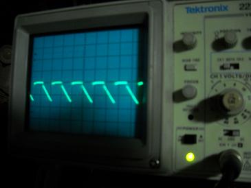
just because your a GURU or forum administer does not mean your always correct :) |
||||
| Warpspeed Guru Joined: 09/08/2007 Location: AustraliaPosts: 4406 |
I highly recommend the purchase a couple of those International Rectifier isolated gate drivers. They are fast, designed to do that exact job, and and will allow both ends of your MOSFET to safely go up to several hundred volts without any problem at all. Cheers, �Tony. |
||||
| govertical Guru Joined: 11/12/2008 Location: United StatesPosts: 383 |
Hi, is it possible to have a transistor configuration to oscillate Vgs? When point �A� is enabled the voltage at point X will be 2 times the battery voltage. MOSFET source is always at the plus value of the battery voltage and is consider ground with respect to Vgs. The MOSFET requires 10 volts at the gate to turn on. Use a resistive voltage divider to create a high and low side of the voltage at point X. Configure a transistor circuit on the high side of the voltage divider to provide 10 volts to gate. I do not have a lot of experience with transistor circuits, comments are welcome. 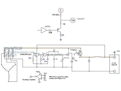
just because your a GURU or forum administer does not mean your always correct :) |
||||
| Warpspeed Guru Joined: 09/08/2007 Location: AustraliaPosts: 4406 |
There are quite a few different ways to go about this, and every single one, has some disadvantage or other. 1/ Use a proper commercial purpose designed isolated high side gate driver chip. 2/ Drive the gate through a pulse transformer. This can work well, except you will be quite limited to how far you can swing the PWM either side of an even 50/50% duty cycle. 3/ Design (or purchase) a small switching supply to generate a fully floating isolated 12 volt power source, and use a high speed opto isolator to couple the PWM to a fully floating gate driver circuit. 4/ Use a P channel power mosfet, instead of a much more desirable N channel power mosfet, and build a level shifting circuit using a high voltage bipolar transistor to reference the gate drive to the incoming high positive voltage. Cheers, �Tony. |
||||
| govertical Guru Joined: 11/12/2008 Location: United StatesPosts: 383 |
Hi, project update. The test circuit is using to separate bench power supplies, one to power the 555 and the IR2117 and the other supplies power for Vin and acts as the PMA. The load is a 12 volt tail light and the oscillator is at 10 kHz. I had a lot of problems because the bench power supplies that I am using are programmable. Once I configured them correctly most of the problems have been solved. The output from the 555 oscillator has a severe ringing that is transferred to Vs of the mosfet. But the boot strap appears to be working with the Vs from the IR2117 connected to Vs of the mosfet and the mosfet is turning on and off. I am currently searching for away to supply the IC�s with Vcc. I am not sure if I should use a 12 volt linear regulator from the 12 volt battery bank or if there is a method to use the large input capacitor at Vin. The voltage at Vin can range form 0 to over 200 volts open circuit and I do not know how fast the buck converter will drain the cap at Vin when the mosfet is oscillating. Comments are welcome. output of 555 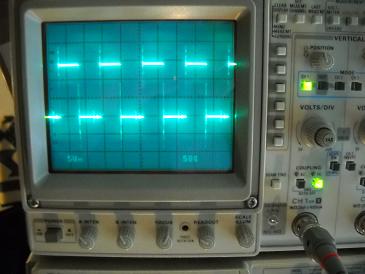
Vs of IR2117 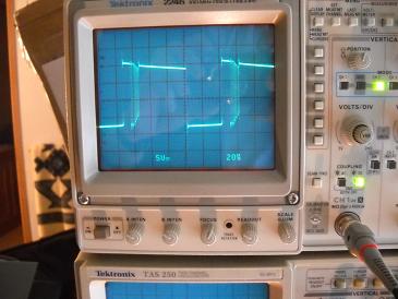
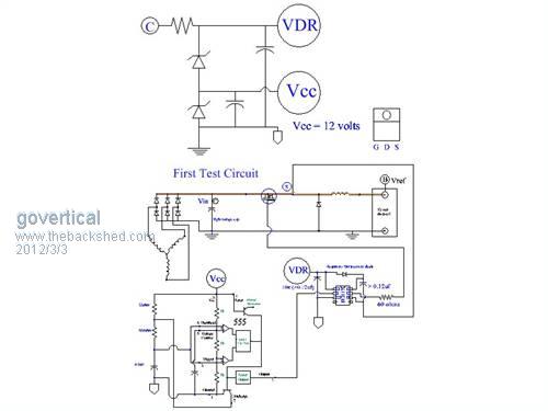
just because your a GURU or forum administer does not mean your always correct :) |
||||
| Warpspeed Guru Joined: 09/08/2007 Location: AustraliaPosts: 4406 |
Just use the +12v from the battery to power the 555. The circuit will not be able self start without a battery connected, which is only going to be an inconvenience during testing. Once built properly and installed with a battery it will work fine. I suggest you decouple the battery voltage with a resistor, maybe 100 ohms or something, and a decent electrolytic capacitor. If you want to run the 555 off the high voltage side, that would be possible with a suitable high voltage regulator, such as this : You might need about a 15v zener to get around +12v output. 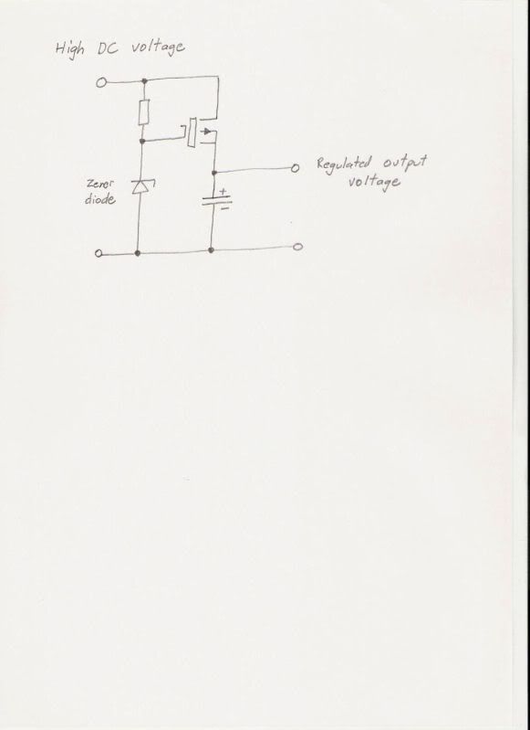 Cheers, �Tony. |
||||
| Warpspeed Guru Joined: 09/08/2007 Location: AustraliaPosts: 4406 |
I suspect you may have some grounding issues. Make sure the ground connection between the 555 and IR2117 is very short and direct, and that the 555 has a good high frequency tantalum decoupling capacitor between supply and ground close to the chip. There are some very fast waveforms here, and ringing is quite likely, unless everything is very close, tightly packed, and properly bypassed with suitable capacitors. Much easier to do on a proper circuit board than the typical prototype birds nest of clip leads with various parts spread across the work bench. The circuit is fine, it probably just needs tidying up a bit, and you will then have some beautiful fast perfect square waves to look at. Cheers, �Tony. |
||||
| govertical Guru Joined: 11/12/2008 Location: United StatesPosts: 383 |
video of wave form Hi, video shows manual operation of PMA and buck converter to a resistive load. The mosfet is turning on during the off cycle of the IR2117. Is there a solution to this problem??? Comments welcome. close up of wave form just because your a GURU or forum administer does not mean your always correct :) |
||||
| Warpspeed Guru Joined: 09/08/2007 Location: AustraliaPosts: 4406 |
Try putting some reasonably decent load on the buck regulator, it should then work fine. If that is the problem, I have a fair idea what is going on. Cheers, �Tony. |
||||
| govertical Guru Joined: 11/12/2008 Location: United StatesPosts: 383 |
Hi, I switched the load to a 50 watt light. The waveform is the same and the PMA is more difficult to spin. just because your a GURU or forum administer does not mean your always correct :) |
||||
| Warpspeed Guru Joined: 09/08/2007 Location: AustraliaPosts: 4406 |
The problem appears to be that the MOSFET is having great difficulty turning on, and that the problem is cycling in and out at a rather low frequency. This can only be caused by the voltage pump and charge storage capacitor that powers the isolated dc voltage to run the isolated gate drive circuit. 
This charge storage pump consists of the diode connected from +12v to VB on the IR2117 chip, the energy storage capacitor between VB and VS, and the circuits output load between VS and ground. When the MOSFET is off, VS is supposed to be held at ground potential by whatever load is on the output of this circuit. The capacitor between VB and VS then charges up to +12v less the small forward voltage drop through the diode. This cannot happen unless the voltage on VS goes right down to ground when the MOSFET turns off. Unfortunately there is nothing in this circuit to do that, except the flyback voltage across the buck regulator choke. The presence of a battery on the output also makes this problem a bit worse. The choke flyback voltage should be more than sufficient to do this, when some small load is placed on the buck regulator, and if the choke is working properly. You still have a problem with that nasty ringing, and I suggest you need to first fix your grounding to get rid of that, and also look at what is happening with the voltage on the source of your MOSFET. That too is probably doing something rather strange. The VS pin on the IR2117 absolutely must momentarily go right down to ground when the MOSFET turns off, so that the capacitor between VB and VS has a fighting chance to charge up to the full +12v during each "off" period. You can also try making the charge pump storage capacitor a bit larger (1uF tantalum), and the diode must be a fast recovery type, (maybe UF4004 or similar). A slow low speed power rectifier diode such as a 1N4004 is not going to work in that position, especially with the charge storage capacitor being as small as it is. What are you using for the buck regulator choke ? Cheers, �Tony. |
||||
| govertical Guru Joined: 11/12/2008 Location: United StatesPosts: 383 |
Hi, http://www.fairchildsemi.com/an/AN/AN-558.pdf Fig. 28 of the .PDF file is the only reference I could find that talks about ringing when the gate driver turns offs. It does suggests a solution. The ringing is present with no input voltage, which suggests it is coming from the oscillator, I am searching for a more stable oscillator circuit that can provide a variable duty cycle. Should Vload be turning on and off ? I made a new drawing of the circuit. PMA ground is not connected to the power supply ground. The power supply is powering only the IC�s. I order some fast recovery diodes, I did not have any so I tried a switching diode. The output inductor is 46 turns of 18 AWG with a center hole radius of 0.73 inches and a height of 0.34 inches. Measured resistance is 0.14 ohms. It is very possible that it is not the correct inductor for the circuit, it was made using best guess numbers. Thank you for taking the time to help me it is greatly appreciated. Short video of Vg and Vload: Vg&Vload 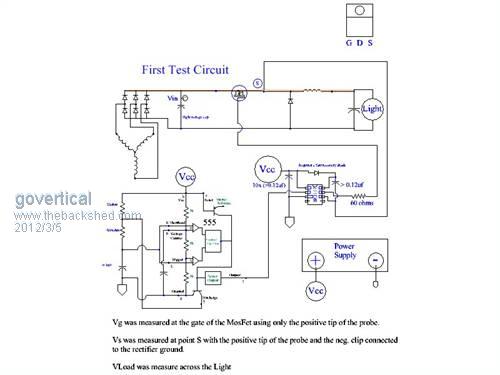
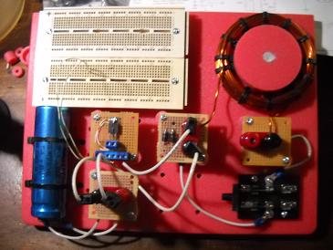
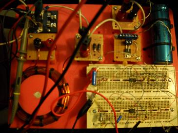
Should Vload be turning on and off or should it be a constant? just because your a GURU or forum administer does not mean your always correct :) |
||||
| Warpspeed Guru Joined: 09/08/2007 Location: AustraliaPosts: 4406 |
V load will only be constant if there is a battery or a very large output filter capacitor connected to the output of the choke to hold the voltage constant. Depending on the nature of the connected load, and the relative inductance of your choke, the output voltage may contain considerable ripple. Cheers, �Tony. |
||||
| govertical Guru Joined: 11/12/2008 Location: United StatesPosts: 383 |
Hi, I connected the grounds and the results are the same. At this time I am replacing the 555 with a different oscillator circuit to determine if it will remove the ringing during the off state of the MosFet. With the new oscillator I should be able to vary the duty cycle. I will post results in a few days. http://pcbheaven.com/circuitpages/Triangle_Wave_Generator/ http://www.pcbheaven.com/circuitpages/Voltage_Controlled_PWM _Generator/ 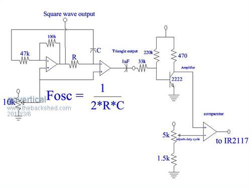
just because your a GURU or forum administer does not mean your always correct :) |
||||
| govertical Guru Joined: 11/12/2008 Location: United StatesPosts: 383 |
Hi, I found a reference to the problem on page 8 and 9. http://www.nalanda.nitc.ac.in/industry/appnotes/IR/ASSETS/TE CHDOCS/APPNOTES/An978.pdf It recommends increasing the boot strap capacitor to a valve greater than 0.47 uf. I will post results when available. just because your a GURU or forum administer does not mean your always correct :) |
||||
| Page 1 of 5 |
|||||
| The Back Shed's forum code is written, and hosted, in Australia. | © JAQ Software 2026 |