
|
|
Forum Index : Electronics : Inverter building using Wiseguys Power board and the Nano drive board
| Page 1 of 35 |
|||||
| Author | Message | ||||
| KeepIS Guru Joined: 13/10/2014 Location: AustraliaPosts: 2177 |
The focus of this thread is to help forum users who may be new to Inverters and unsure of where to start with building one, hopefully showing how easy most of it is. There are many boards and variations on this forum, and this build is a smaller Inverter of the same design as my main inverter. I’m using the same fabulous Power board design by Wiseguy, but the control will be the Nano controller design from Poida. I’m going to take some very detailed photos during the build, I hope to show just how easy this power board is to build. I’m not going to go off topic and discuss any variations or much technical info. That has been done to death on this forum and all information is here on the forum if you search or read. I won’t be covering the Toriod or Chokes – all done to death elsewhere on the forum. First the Power Board: This power board has FOD3180 opto-coupler drivers on the FET power board in close proximity to the FETs, it uses Warpspeeds suggested cross coupled opto drive method and Wiseguy has used isolated gate driver power supplies for the high and low side. This has solved most of the problems with PWM spikes and high current loading getting through common ground connections and into the FET drive circuitry. I should also protects all the driver components in the event of a FET failure. Dead time: This is handled by a 1nF cap across the LEDs of the gate drive optos and controls the dead time for each half bridge, with a 1nF cap and series resistance of 120 ohm it gives around 120 nanoseconds with the available drive voltage. The gate drive buffer is essentially an emitter follower current driver with an active gate clamp in the absence of power. Negative three volts is applied to the Low side FETs for both lower legs of the Bridge, they share the same 15v bias supply. I ordered most of the parts from www.lcsc.com, most forum users have found the parts to be genuine as have I. The power board circuit: There are various bias supplies and negative bias options, but to keep it simple I’m showing only the circuit and the parts that I used in this build. 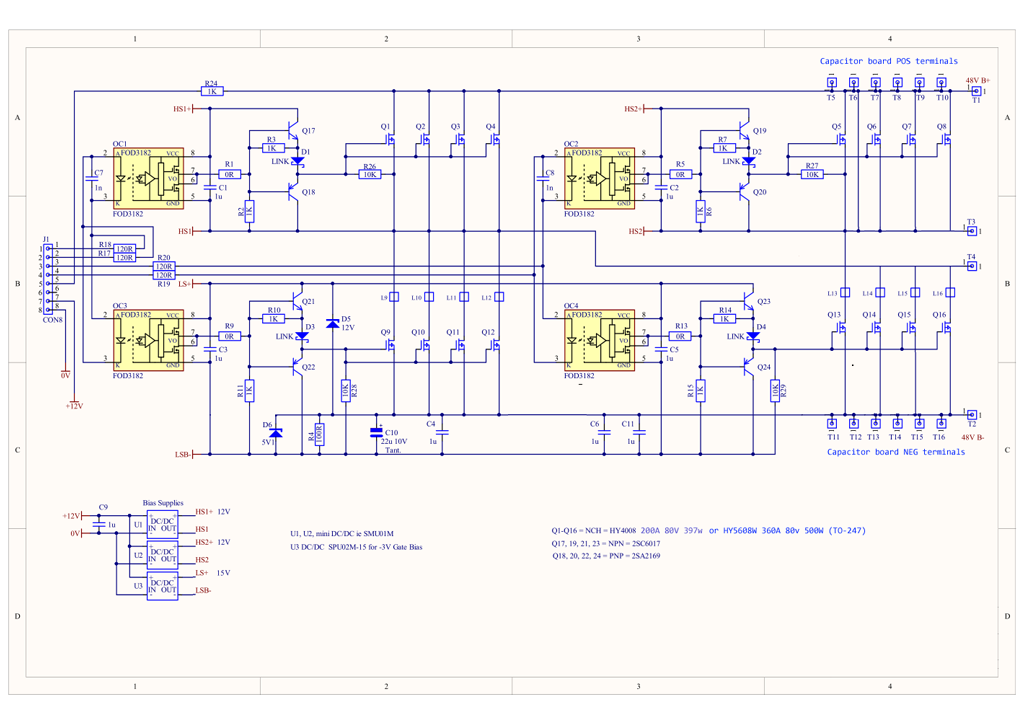 I will provide a detailed circuit and more parts info along the way. The next few posts will only be on the Power board. The Nano driver board will follow. This power board is a proven high power running inverter design, you simply select or wind your Toriod and connect. The board layout, FET mounting and Heatsink mounting is very simple and clean. Below: The finished power board mounted on an old heatsink, the two small Cap boards removed. The Capacitor boards simply screw on and off easily. The 3 terminals top and bottom on each side of the main board are the Connection / mounting posts for the Cap boards. 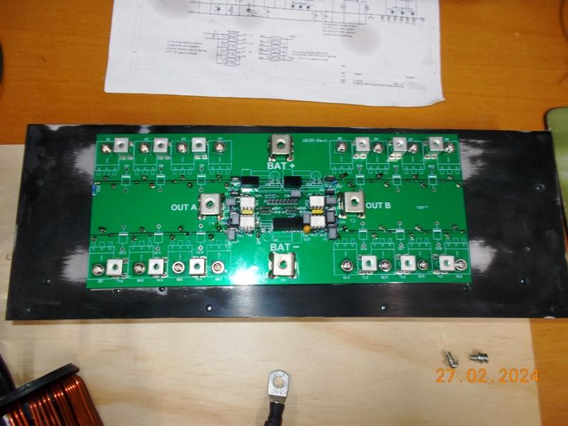 Detailed photos to follow in the next few posts. NANO:Inverter V 8.2ks - Linux AvrDude GUI script V4.1 |
||||
| -dex- Senior Member Joined: 11/01/2024 Location: PolandPosts: 104 |
I also started building a wiseguy power board. What I can say for myself is that when soldering large M6 connectors, it is worth using something more than a standard soldering iron. The board is 2 oz thick copper, and the connectors mounted on the copper spout receives a lot of heat when soldering. I used a powerful 400W soldering iron, soldering it goes like piece of cake   |
||||
| KeepIS Guru Joined: 13/10/2014 Location: AustraliaPosts: 2177 |
These show the component layout and the three small isolated DC-DC supplies. 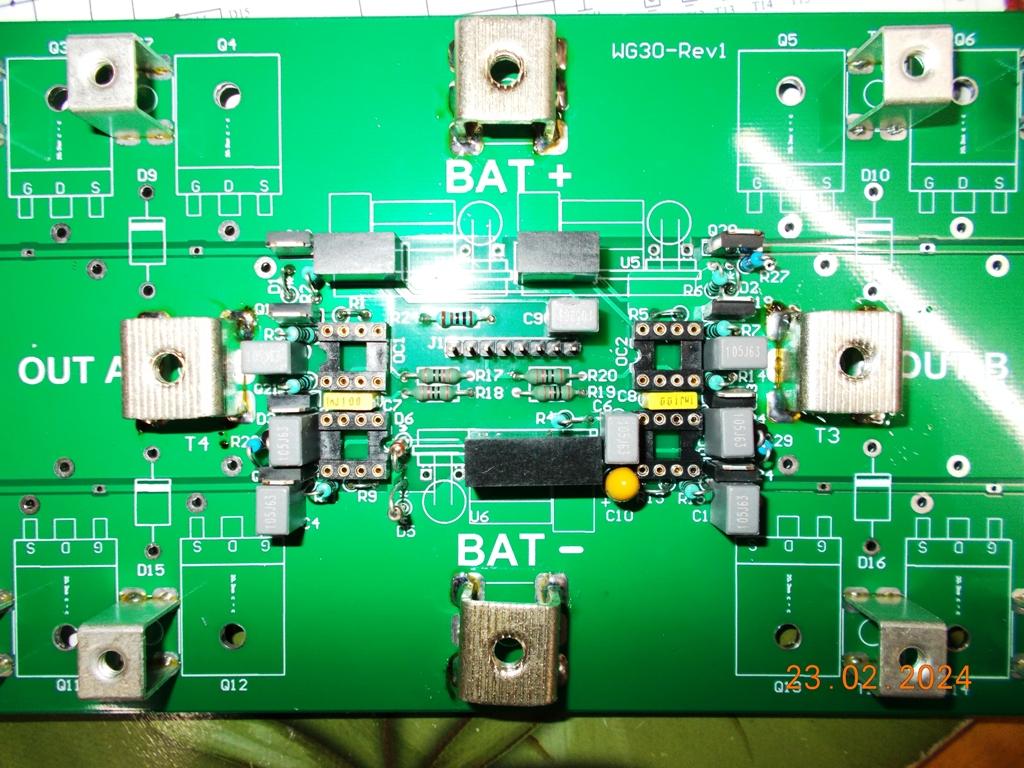 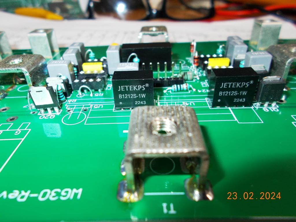 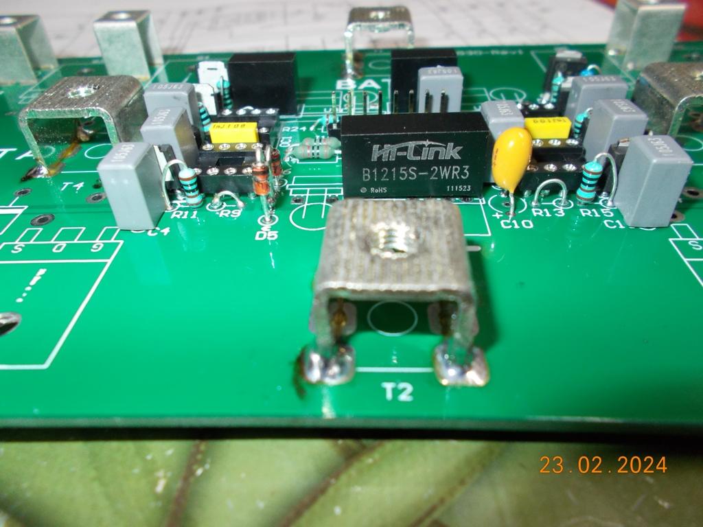 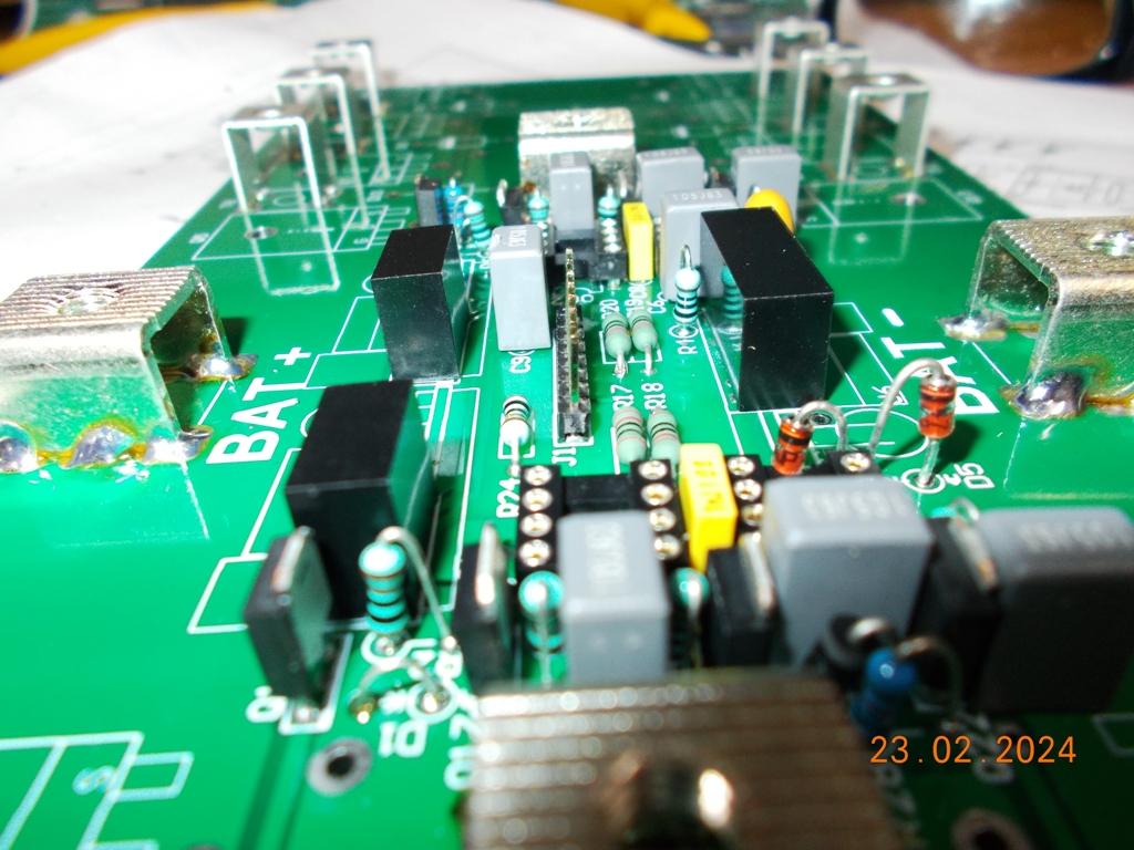 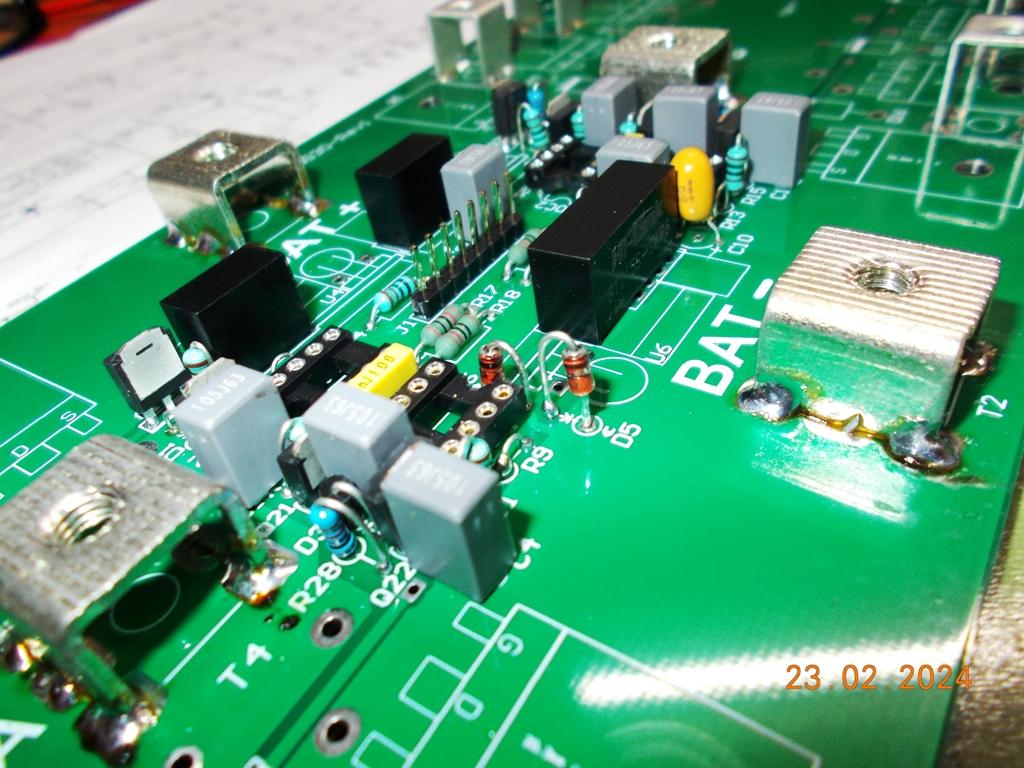 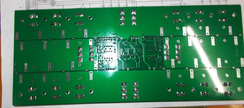 FET mounting to follow. NANO:Inverter V 8.2ks - Linux AvrDude GUI script V4.1 |
||||
| KeepIS Guru Joined: 13/10/2014 Location: AustraliaPosts: 2177 |
In this board I used a thick terminal pin to solder the Drain and Source legs of the FETS. This makes it simple to replace FETS without damage to the PCB in the event of a Failure. I did not install the optional small ferrite chokes. The Pin I used is shown in the center of the PCB. 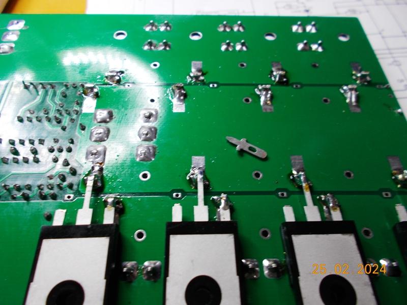 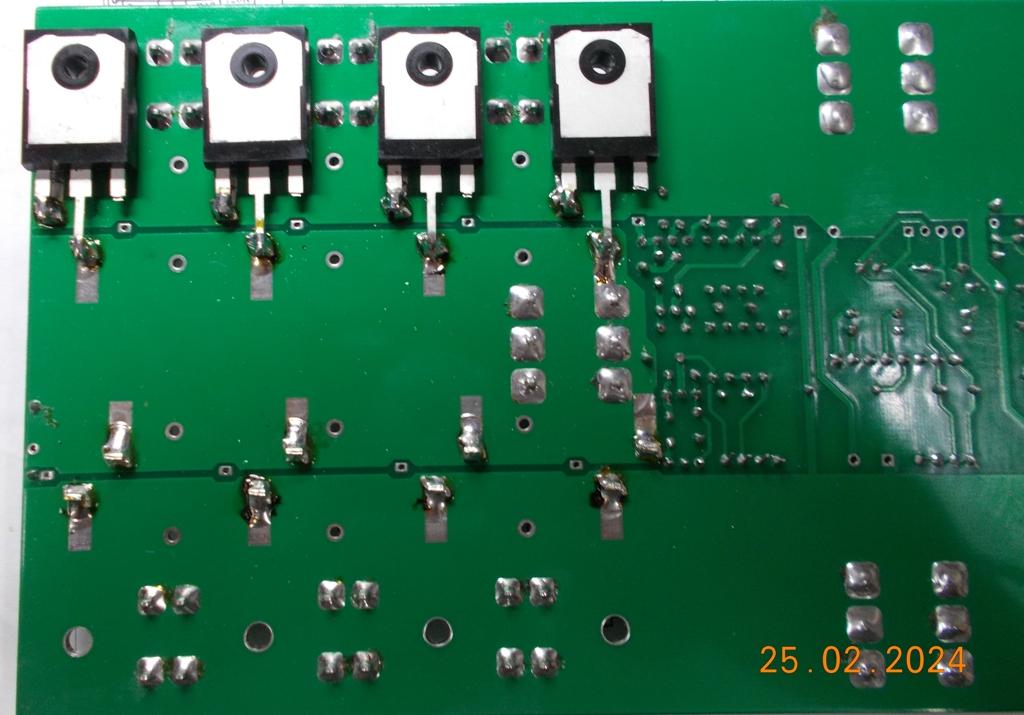 The Gates are connected via a 2.2 ohm (2R2) resistor, this makes it simple to remove the FETs if needed. These resistors is not shown on the circuit for clarity. 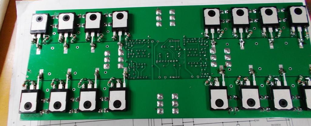 NANO:Inverter V 8.2ks - Linux AvrDude GUI script V4.1 |
||||
| KeepIS Guru Joined: 13/10/2014 Location: AustraliaPosts: 2177 |
The main terminals are easily soldered with a standard good quality soldering station and a thick tip. In keeping with the goal of keeping this simple, I do not expect people to have to purchase extra equipment to build the board. There are a few ways to mount the board to the Heatsink. For this build I used an old Heatsink from a scrapped GT Solar inverter. I positioned the board so that all FET holes were away from any old mounting holes in the heatsink. You can purchase a 3mm Tap a 2.5mm drill and cutting oil from various hardware outlet. It just takes a bit of time to tap the 16 holes. FET Insulators: I purchased two meters of thermal mat, you can see the gray mat between the Fets and the heatsink. I'll look up the source and post a link. This is this same mat I used on my big inverter build, it's brilliant. You can of course use standard individual FET heat transfer insulators. 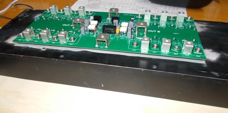 There are other ways to get around having to tap the heatsink by using flat intermediate aluminum heat transfer bars. Both Wiseguy and I have used this method before. I will post more on this shortly. Once again, please don't post other mounting methods until I have finished posting the build, all that will do is make the build thread confusing for people new to inverter building. I will expand further once I have the basic layout and pictures uploaded. Thanks. NANO:Inverter V 8.2ks - Linux AvrDude GUI script V4.1 |
||||
| KeepIS Guru Joined: 13/10/2014 Location: AustraliaPosts: 2177 |
The information was posted by Wiseguy and I hope he doesn't mine me posting it here. This is the method that he used to avoid tapping 16 x 3mm holes. 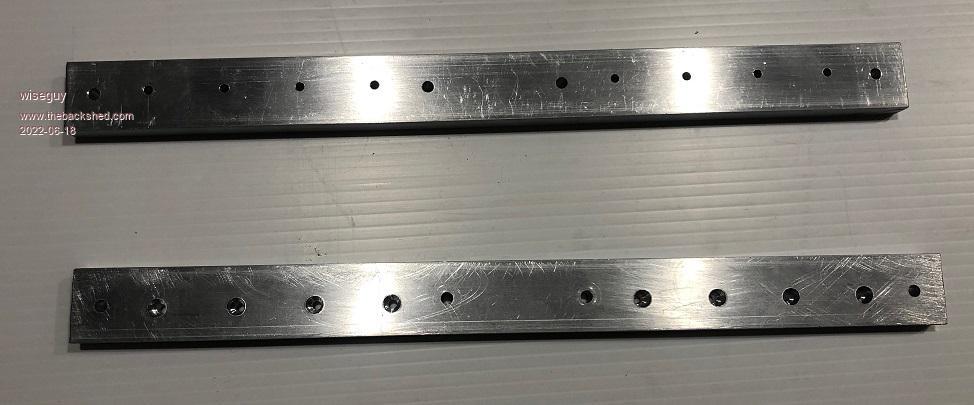 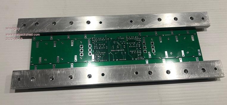 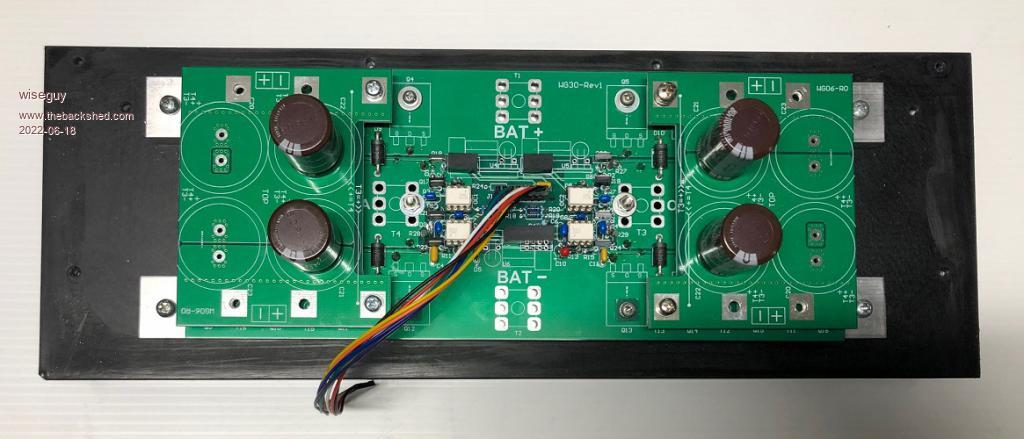 Note the CAP boards are shown in the photo above. There are two types of board, one is for solder in Caps shown above, and another is for screw in Caps. NANO:Inverter V 8.2ks - Linux AvrDude GUI script V4.1 |
||||
| KeepIS Guru Joined: 13/10/2014 Location: AustraliaPosts: 2177 |
This is the FET Heatsink interface for my big inverter. I made it this way to get maximum heat transfer efficiency. The Heat transfer bars are cut in half for the Lower bridge FETS, this allows the FETS to be mounted directly to the heat transfer bars without any insulation, giving maximum heat transfer from the FETS under very high power loads and High transient current (heat) demands. The upper heat bar can be one piece as they share a common +48V rail connection, I used two separate bars as I did not have one long bar. These bars came out of old GT inverters. Once again there is an insulator mat between the Heat bars and that huge Heatsink. I have found that this heatsink might be a bit of overkill, what you can't see here is the massive fin size area and thickness of that heatsink. The heat transfer bars present a large surface area to the insulator mat / heatsink interface and ensure maximum efficient heat transfer through the insulator mat into the Heatsink. In my case the Heat transfer bars are again 3mm tapped. 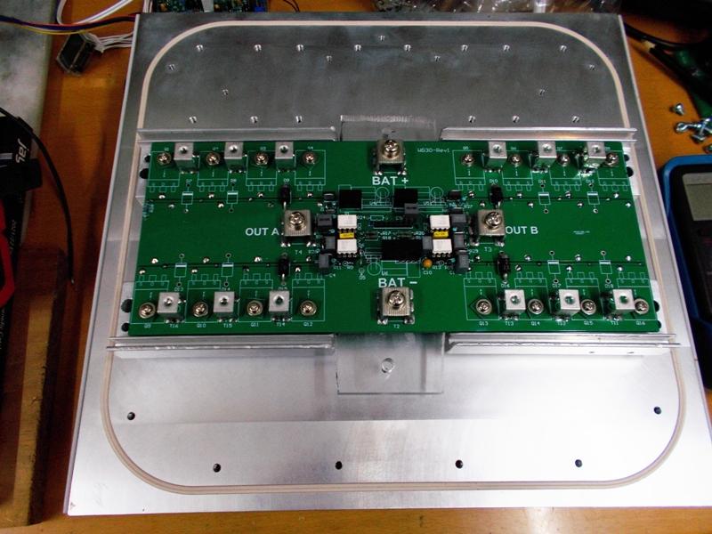 Old pix of a test setup with small value Cap boards. 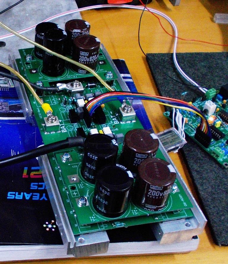 . Edited 2024-03-05 11:40 by KeepIS NANO:Inverter V 8.2ks - Linux AvrDude GUI script V4.1 |
||||
| KeepIS Guru Joined: 13/10/2014 Location: AustraliaPosts: 2177 |
The release of the latest Nano Controller, this is a collaboration between Wiseguy and Poida and was just announced. New Nano This is the new controller I'll be using for the Power board. I will finish off the power board build with a description of the Toriod and the Chokes that I will be using, and more details of the FET mounting hardware. The following is some of the parts used, I was having trouble finding stock of some items, especially the Buffer transistors, Wiseguy addressed this in his release so I have included that info here. Cap board screw to PCB7XM4 metal "U" M4 threaded x 4 solder pin standoffs on the main PCB. Total of 12 needed. PCB-5 M6 with screws X 4 for Power and Toriod connection. From www.lcsc.com Minium amount for one board. Buffer transistors: MJD45H11-1G X 4 2SD1804L-T-TM3-T X 4 The TO251’s types above are now very hard to find, similarly rated SOT223 surface mount transistors that use the same pin spacing as the TO251s can have the 3 (short) legs inserted into the existing PCB pad holes and soldered. LCSC has the SOT223 PNP and NPN versions for the buffers which are ~30c ea and have continuous current ratings of ~5A and peak current ratings of ~ 15/20A so the overall cost is low. HY5608W Power FET X 16 (360A @ 80V 500W rating) FOD3182V Opto couplers X 4 (none at LCSC but available elsewhere) 2 x B1212S-1W PCB SIP DC/DC 1W modules 1 X B1215-2W I used a HI-LINK HLK-B1215S-2WR3 but only 8 showing in stock at lcsc.com LCSC has stock of various brands listed here DC-DC modules The spacing between the two input and two output pins of the 2W 15v units is slightly different on some, however it's only a matter of drilling two tiny holes for the input pins next to the existing pads, they fit and solder perfectly. A lot of these components are relatively low cost and it pays to order more than needed. Edited 2024-03-06 09:06 by KeepIS NANO:Inverter V 8.2ks - Linux AvrDude GUI script V4.1 |
||||
| KeepIS Guru Joined: 13/10/2014 Location: AustraliaPosts: 2177 |
While I think of it, one piece of workshop equipment I would recommend as almost a Must Have, is a current limited Variable Power supply to power the inverter through the testing and setup stages. Being able to power up the inverter (initially without the cap boards) with a current limit of 300mA for the initial power up will save you a world of pain if something is not right. The unit I use can allow around 230 Watts of Inverter load to tested. It allows you to slowly wind up the voltage to the inverter during testing, and "almost" eliminating any damage if there happens to be a fault. More about power up and testing later. I posted about this unit here Power Supply The Unit has increased in price to $127, still here on Amazon and in stock in AU. 0-60V 0-5A 3 Digit NANO:Inverter V 8.2ks - Linux AvrDude GUI script V4.1 |
||||
| KeepIS Guru Joined: 13/10/2014 Location: AustraliaPosts: 2177 |
FET to Heatsink mounting: The screws for the high side FETs must be insulated from the positive plane with a small TO220 mounting bush. You can also purchase TO220 insulating washers (instead of the Heat mat that I use) and bushes in packs of 10 or 20 for a few dollars in AU. 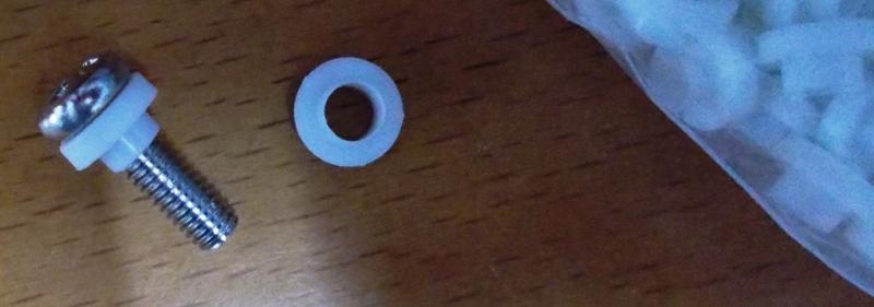 I use a little square fiber pcb washer on top as well, these come as part of each cap board, just need to cut them off. The lower side screws don't normally need to be insulated as they connect -48v to the heatsink, however in my case I used insulating bushes here as well, so the heatsink is fully insulated from the inverter power planes. My reasoning is that if something accidentally touches the heatsink, nothing gets shorted out or blown if the heatsink is not mounted to a metal chassis and not connected to anything. But that's just me - do as you please. There is more spacing between the Gate resistors and the insulating mat that it appears in the photo, optical illusion. Here you can see the screw insulating bush and the square fiber pcb washer on top. 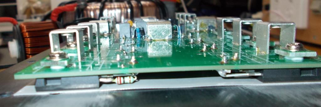 BTW Having the heatsink grounded or floating does not appear to make any difference to the Power board waveforms with respect to noise. NANO:Inverter V 8.2ks - Linux AvrDude GUI script V4.1 |
||||
| KeepIS Guru Joined: 13/10/2014 Location: AustraliaPosts: 2177 |
I finally found the receipt for the Thermal Silicone mat, however it's no longer available from this source, but it's what I'm using. BM120 Sil-Pad Coated Fiberglass 0.3mm*300mm*1m Thermal Silicone Pad for Heat Sink. Heat Transfer Silicone mat. Should be easy to find elsewhere. EDIT: A bit dear but give you an idea. Easily do a full heatsink. RS Components . Edited 2024-03-06 11:40 by KeepIS NANO:Inverter V 8.2ks - Linux AvrDude GUI script V4.1 |
||||
| wiseguy Guru Joined: 21/06/2018 Location: AustraliaPosts: 1296 |
Thanks for your post on putting one of these together it saves me a bunch of work. With regard to testing the inverter and controller cards after building them, I have a test routine that starts typically with 30mA current limit and 12V. As various tests and results are obtained we can increase voltage and current to the increments in the test procedure. As part of the total post here I will include the test procedures for controller and power pcbs along with bill of materials etc. I am pretty good at not letting the smoke out as things are brought to life by determining very early if the units are working ok. When connected to a Power board there are some further tests, again with low voltage starting at 0V and increasing to 6 I think (- at work cant check right now) and 0.1A current limit increasing to 1A before choke and transformer are connected. The power PCB can be powered from 0-50V with the sinewave increasing proportionally to voltage increase and if all is well it will begin to regulate at ~230V at around 45V if all is well. If at first you dont succeed, I suggest you avoid sky diving.... Cheers Mike |
||||
| KeepIS Guru Joined: 13/10/2014 Location: AustraliaPosts: 2177 |
Thank Mike, that cover most and more of the test write up I was planning. I'm limited to how long I can sit without one leg up in the air, almost back to normal now though. I've been a bit slow to get this started over the past two weeks because of that. I'll leave you to post the testing procedure for everyone, especially since it sounds like it will include the new Nano R6 controller testing and power up. NANO:Inverter V 8.2ks - Linux AvrDude GUI script V4.1 |
||||
| KeepIS Guru Joined: 13/10/2014 Location: AustraliaPosts: 2177 |
FYI - This is the single Toriod that I will be using. This Toriod is from an old Aerosharp GT inverter and is rated at 2kW (in a sealed case). I unwound the secondary and wound 26 turns of 8G cable for the testing. This will be replaced with heaver gauge once everything is finalized. With cooling, the Toriod could easily run at around 4kW for a few hours. The Choke is a test choke, standard item from China and current good for around 180A before it runs out of inductance and becomes a long piece of wire. This inverter will have two chokes the same size and configuration as my main inverter - Two 6 stack SI toriod rings with 4 turns of heavy gauge cable each. These can be seen on my main build. Below: The small Variable 0-60v power supply is the white box next to the DSO. Behind the heatsink is the old Driver board, it will be replaced with the Nano R6. Even in this state it can start very high power loads and run at over 5kW easily when on Batteries. I've tested this toriod before at those levels. 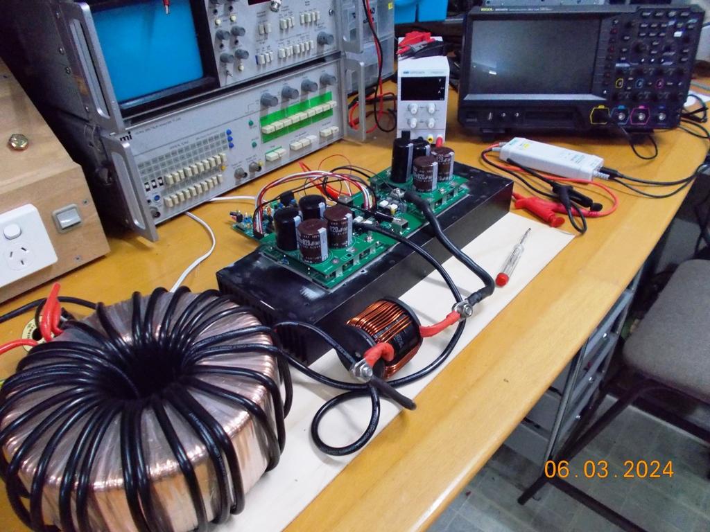 NANO:Inverter V 8.2ks - Linux AvrDude GUI script V4.1 |
||||
| KeepIS Guru Joined: 13/10/2014 Location: AustraliaPosts: 2177 |
At this stage if anyone has any input or question about the Power board build, please feel free to post them here. This will free up the thread to post the Controller build when I start building it and posting in the final part of the build.  NANO:Inverter V 8.2ks - Linux AvrDude GUI script V4.1 |
||||
| KeepIS Guru Joined: 13/10/2014 Location: AustraliaPosts: 2177 |
I wanted to test the the inverter power board with and without the Ferrite Beads shown in the circuit. They do indeed make a big difference, I would recommend fitting them. The beads are fitted in the Drains of Q9 to Q16 in the circuit shown in the first post, beads are marked as L9 to L16 - not very clear in the circuit. The beads I used are Electus (Jaycar?) LF1251 or FX1115. They are about 4.2mm diameter x 5mm long the hole in the center is ~ 1.3mm. They need to be small as indicated and just fit over the Drain (center pin). FYI: Found an old pix from Wiseguy showing the Ferrite bead. 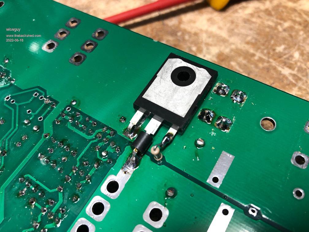 . Edited 2024-03-08 13:37 by KeepIS NANO:Inverter V 8.2ks - Linux AvrDude GUI script V4.1 |
||||
| -dex- Senior Member Joined: 11/01/2024 Location: PolandPosts: 104 |
What about the remaining FETs Q1-Q8? In the circuit diagram posted before, they also have ferrite beads drawn on them. Edited 2024-03-08 21:33 by -dex- |
||||
| KeepIS Guru Joined: 13/10/2014 Location: AustraliaPosts: 2177 |
An earlier version of the PWR board showed them on Q1 to Q8 as well, there was an earlier circuit during the first design stages that had the Beads in the Gates. There was a lot of work carried by Wiseguy and Poida investigating exactly what was happening with the FETS, Ferrite beads and ringing in inverters, and they were moved to the FET Drain. If you can fit them by all means try them, in may case everything looks good now, much better then the typical inverter power stage ringing. Now the ferrite beads that Wiseguy and I use will not fit over the wide part of the FET leads. There is also limited space on Q1-Q8 to fit them to the Drain, that lead is bent straight down after the wide shoulder and onto the +48v power plane just below the FET body. Also the Q1-Q8 drains connect to the power supply +48v rail, this has a lot less HF switching noise compared to the Choke / Toriod input terminal T4 for Q9 to Q16. Fitting just the low side Ferrite-beads made both the HI and LO side PWM output very clean and almost identical in my testing when measured with a 380mHz bandwidth DSO. You will also notice that I did NOT show Diodes D7 to D18. The original design was using HY4008 FETS, however I had a failure of one of those Diodes when using HY5608W. NOTE: That happened under an extreme almost 30kW pulse condition, I really brutalized that the Big inverter and Wiseguys power board during the first 6 month of torture testing. The Diodes turned out to be a weak link and underrated compared to the body diodes in the HY5608W, which are the recommended Power FETs to use. Wiseguy and I decided to leave them out as they are not really needed with the HY5608W FET. NANO:Inverter V 8.2ks - Linux AvrDude GUI script V4.1 |
||||
| wiseguy Guru Joined: 21/06/2018 Location: AustraliaPosts: 1296 |
When I made my FET boards I ground a pair of pliers to create the bend of the wide shoulder of the drain leg about half way down its length - very close to the FET. the other Bends are less critical but must be close enough for ~ 4-5mm of the Drain leg to pass through the circuit board. In doing so we ensure the high current is not relegated to flowing through the plating of the inner holes from the top side to solder side. I also made a Jig to bend the Low side FETs D & S legs, note the Drains are short and Sources are long on the Topside and reversed for the low side (Drains long Sources short). This method also will only work when the aluminium interface bar lengths are fitted, as direct fitting to a flat surface will undoubtedly interfere with the bend of the Drain Legs that protrude past the Fets heatsinking face. Also note the gate resistors standing on the edge which is fine with clearance of the bar mounts. If mounting to a heatsink direct they need t lay flat as in one of Mikes earlier pictures. Ok more clearly seen in this picture 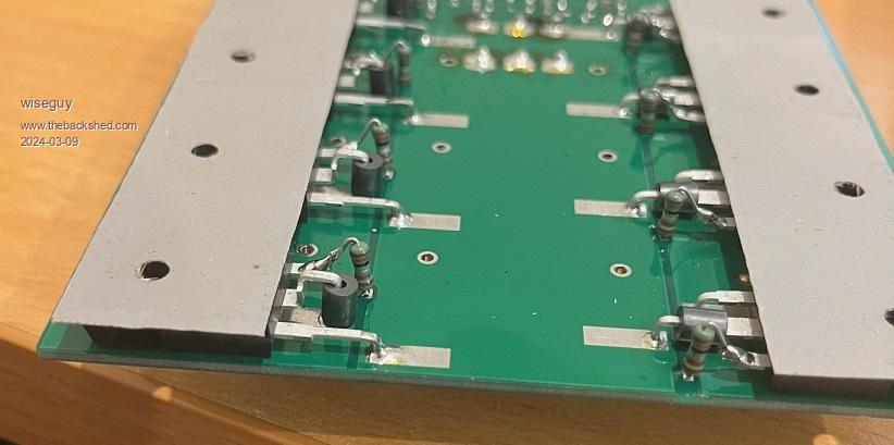 Edited 2024-03-09 10:47 by wiseguy If at first you dont succeed, I suggest you avoid sky diving.... Cheers Mike |
||||
| KeepIS Guru Joined: 13/10/2014 Location: AustraliaPosts: 2177 |
NANO:Inverter V 8.2ks - Linux AvrDude GUI script V4.1 |
||||
| Page 1 of 35 |
|||||
| The Back Shed's forum code is written, and hosted, in Australia. | © JAQ Software 2026 |
