Notice. New forum software under development. It's going to miss a few functions and look a bit ugly for a while, but I'm working on it full time now as the old forum was too unstable. Couple days, all good. If you notice any issues, please contact me.
Solar Mike Guru Joined: 08/02/2015 Location: New ZealandPosts: 1124
Posted: 04:32am 15 Jan 2024
Copy link to clipboard
Print this post
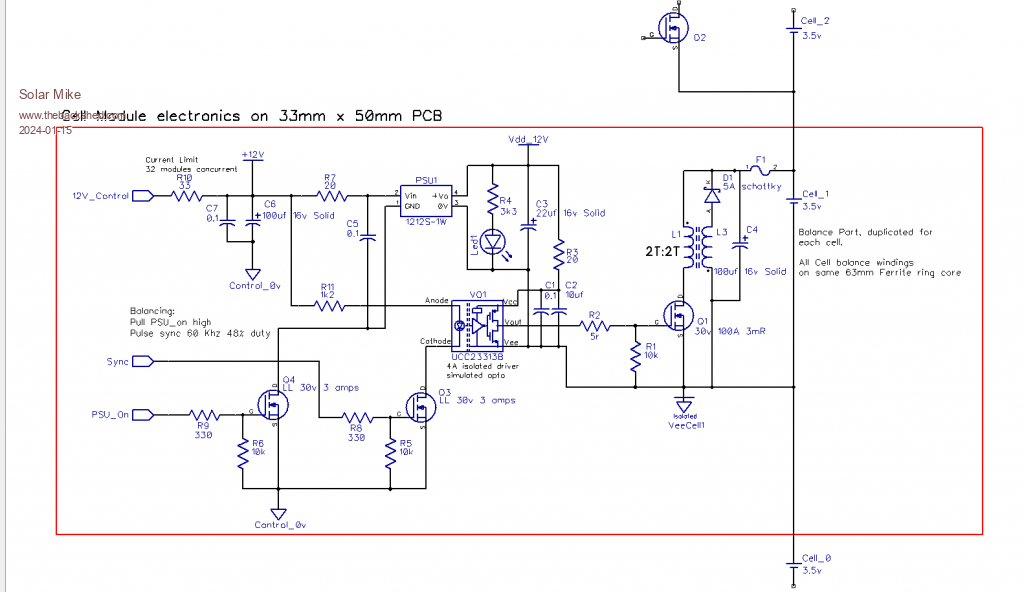
Thought I would have a go at building an inductive battery cell balancer, this one is similar in concept to the design by Warpspeed, but otherwise works in a different manner.
I wanted something that is not specific to a known fixed set of battery cells and could be used with any number of cells by scaling up the design elements in a more modular architecture. Here is the experimental schematic for the electronics for balancing one cell, this is on a small 33 x 50mm PCB that sits on a larger mother board hosting up to 8 balancing modules, a large high mu. ferrite core sits in the middle and links all modules together.
Each module has 2 input signals, one to turn on its isolated mosfet driver bias supply, the other is a PWM input at 60 - 100 Khz and 48% duty cycle; this is used to drive the power mosfet isolated driver in a forward inverter. The mosfet has two 2 turn coils bifilar wound together for best mutual coupling on the ferrite core. One coil driven by the PWM master sync signal feeds power into the core, the other coil acts as a magnetic reset.
As all modules are pulsed at the same instant, they each reflect their cell voltage to the others, effectively placing all battery cells in virtual parallel arrangement, each half cycle. Thus the cells with the highest voltage will feed some energy into those of a lower voltage.
That's the theory anyway, so the only way to test the idea is to build up something and see what happens.
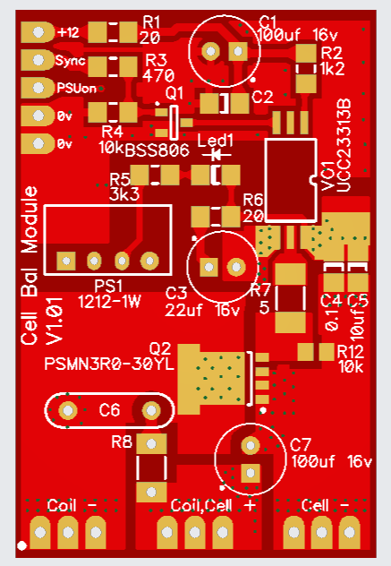
Here is the cell module pcb:
and the host mother board:
I have used a Picaxe 14M2 CPU to measure the balance start voltage and generate the module drive signals, haven't drawn the circuit of this yet, but will do so.
Would also like to have the ability to read each of the cell voltages, so there is room on the pcb to add some extra circuitry to do that in the future.
Next step is get the pcb's made so I can have a play.
Cheers Mike
Murphy's friend Guru Joined: 04/10/2019 Location: AustraliaPosts: 584
Posted: 09:05am 15 Jan 2024
Copy link to clipboard
Print this post
Very nice Mike, your 8 cell board looks a lot neater than the 16 cell board I made to Warpspeeds design.
I made sure to be able to use the heaviest wires possible to each cell and they were all the same length. The design works but any avoidable resistance diminishes the effectiveness when you consider the cell voltage difference may be only a few millivolts. I did have cell fuses to start with but have shorted them with a copper bar to lower the resistance.
I'm interested to see what you come up with regarding cell voltage monitoring. I use a picaxe chip to step 16 telcom relays, each measures the cell voltage for a few seconds before the next cell connects.
Solar Mike Guru Joined: 08/02/2015 Location: New ZealandPosts: 1124
Posted: 11:09am 15 Jan 2024
Copy link to clipboard
Print this post
Yes will be an interesting experiment, will be testing it on a bank of 6V lead carbon batteries and 24V bank of Lifepo4 cells. As you say voltage difference and resistance of wires etc will have an affect on the balance currents. Got to be better than those cheapo balancers available on AliExpress.
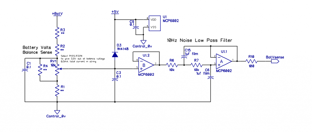
Re monitoring: Optimos solid state dual relay chips and a multiplexer select a cell, its voltage read via INA149 high voltage common mode differential amplifier.
Relays would have a certain contact life ?? quick and easy to do though.
I did start on a 32 cell board, but was going to be expensive to get made, so have opted for the 8 cell version for testing.
Cheers Mike Edited 2024-01-15 21:14 by Solar Mike
Murphy's friend Guru Joined: 04/10/2019 Location: AustraliaPosts: 584
Posted: 01:05pm 15 Jan 2024
Copy link to clipboard
Print this post
I'm using telcom relays (from Altronics), they have the dual double throw contacts required. As each turns on only once every minute or so they have lasted for a few years by now. I had only one failure from 32 relays (2 x 16 cell monitoring) and as they are on sockets its easy to swap a relay.
My balancer uses just a single turn secondary, it was physically impossible to fit two turn secondaries for 16 cells through the hole with the 2mm wire I'm using.
Solar Mike Guru Joined: 08/02/2015 Location: New ZealandPosts: 1124
Posted: 11:50pm 15 Jan 2024
Copy link to clipboard
Print this post
Schematic:
Nothing too complicated with the driver, could have used a simple comparator IC and some sort of 555 oscillator; however the Picaxe's are on hand and prob only 10 lines of code or less to do the logic.
Have used a small mosfet driver IC to drive the balance modules, as eventually there will be 32 of them.
Cannot see any errors, so will fire the gerbers off now.
Cheers Mike
Solar Mike Guru Joined: 08/02/2015 Location: New ZealandPosts: 1124
Posted: 11:35am 18 Jan 2024
Copy link to clipboard
Print this post
Held off on sending the gerbers away until I have something for reading the voltage of the individual battery cells. I want to monitor all cells as they are balancing, even if I attach a DVM and watch it cycle between them.
I have used opti-mos switches in the past to act as a relay that connects to each battery and then measure the voltage with a flying capacitor that gets charged then disconnects from the battery and is then measured in isolation by a common voltmeter; a multiplexer or serial shift register is used to select each mos-switch in turn.
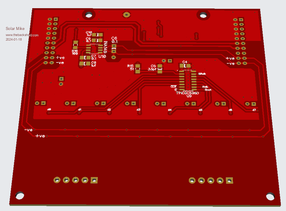
What I have come up with is a 100 x 92mm board with 8 x TLP206 switches to measure 8 battery cells, these ic's are not recommended for new designs by Toshiba as have been superseded, but are readily available on AliExpress quite cheaply in 50 + quantities and are quite small. So 8 of these are selected in turn by a serial high power shift register chip the TPIC6C596, this has open drain outputs and can switch 100ma, so easily turn on each mos switch with 10ma current.
Rather than use a flying capacitor, have opted to measure the cell voltage directly using an INA149, high common mode voltage differential input amplifier with a gain of 1, with +- 12 volt power it can handle 300 odd volts at its input pins, certainly wouldn't purchase these chips off AliExpress.
So here is my first cut at the board, multiple boards can be serially linked by 20p ribbon cable to measure as many cells as desired, additional boards don't require the INA149 components.
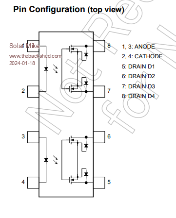
Opti-mos:
Pcb 100 x 92mm Top:
Will add a connector to the balance board so I can talk to this, then send everything away to be made.
Cheers Mike
nickskethisniks Guru Joined: 17/10/2017 Location: BelgiumPosts: 415
Posted: 08:06pm 18 Jan 2024
Copy link to clipboard
Print this post
Another cool project! You started the year with a strong pace . Looking forward to see the schematic, powering your circuit with an isolated dc/dc is another approach to eliminate the flying capacitor.
Solar Mike Guru Joined: 08/02/2015 Location: New ZealandPosts: 1124
Posted: 10:13am 21 Jan 2024
Copy link to clipboard
Print this post
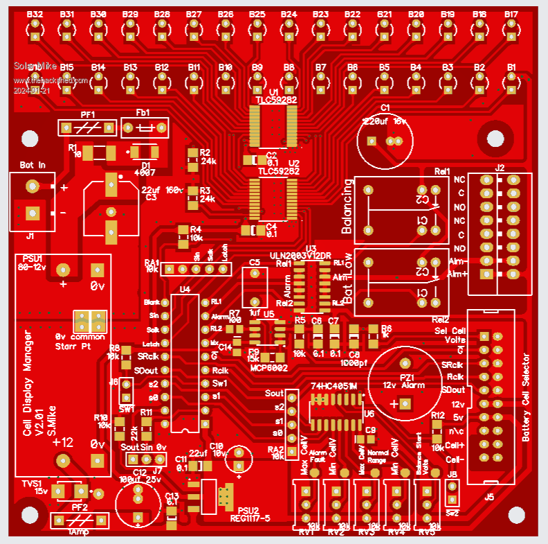
Have been busy, decided to make the balancer board a stand-alone device, it currently has both a total battery voltage sense and an override input switch to begin balancing; it doesn't make a lot of sense to keep adding complexity to that board; after all its a prototype and may not work as expected.
The cell monitor board would work better if it connected to a module that allowed a visual display of each battery in the bank. To keep things simple, a row of leds 32 of them will cover my requirement for a 32 cell 100V bank monitor, leds are placed in two rows and driven by two 16 bit TLC59282 constant current serial input shift register driver chips, these have a universal serial input format similar to the 74HC595 and have a single resistor to set the current for all leds.
Have used the Picaxe20M2 here to provide the two serial stream outputs to the leds and the cell input modules. Added a couple of generic relays, one for "Balancing", other for Battery or cell low, plus a pulldown for an external relay or alarm. The balancing relay can switch on the inductive balancer as required, whilst the other relay can disconnect an "On Load" high power relay or raise an alarm.
Have provided some preset pots to set Cell Min\Max trip points and the balancer start voltage.
Guess what I have got is a simple BMS.
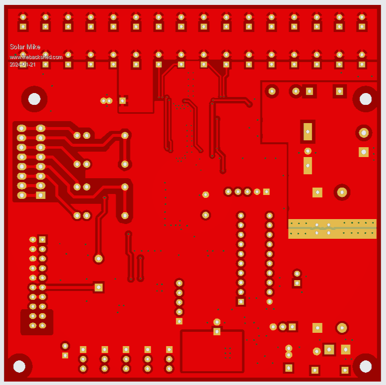
BMS Top, 100 x 100mm:
Bottom:
Cheers Mike
Solar Mike Guru Joined: 08/02/2015 Location: New ZealandPosts: 1124
Posted: 10:19am 21 Jan 2024
Copy link to clipboard
Print this post
Sorry no schematic for that board, pretty simple to work out from the layout.
Cheers Mike
Solar Mike Guru Joined: 08/02/2015 Location: New ZealandPosts: 1124
Posted: 04:20am 29 Feb 2024
Copy link to clipboard
Print this post
After multiple destructive events playing with the 2 cell prototype, I now have a design that works with two 12v battery cells; next is to test an 8 cell version. One thing I can confirm is fast blow ceramic fuses do not protect electronics, cables and wires maybe...
I have 3 x 48v banks of 6v 300AH lead carbon batteries - 8 cells per bank. Three banks are wired in parallel each via 250A DC breakers back to a common 48v load buss, so require three 8 cell balancers. Multiple mppt chargers connect to each bank via their own breakers directly to the battery terminals.
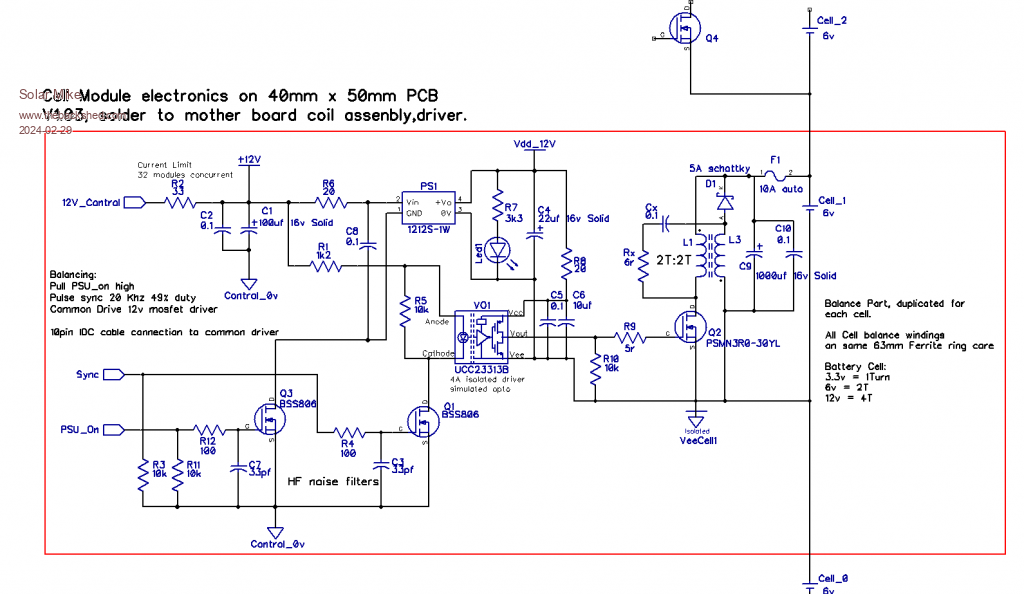
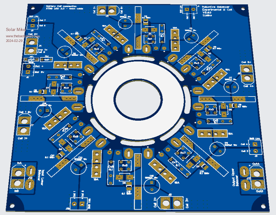
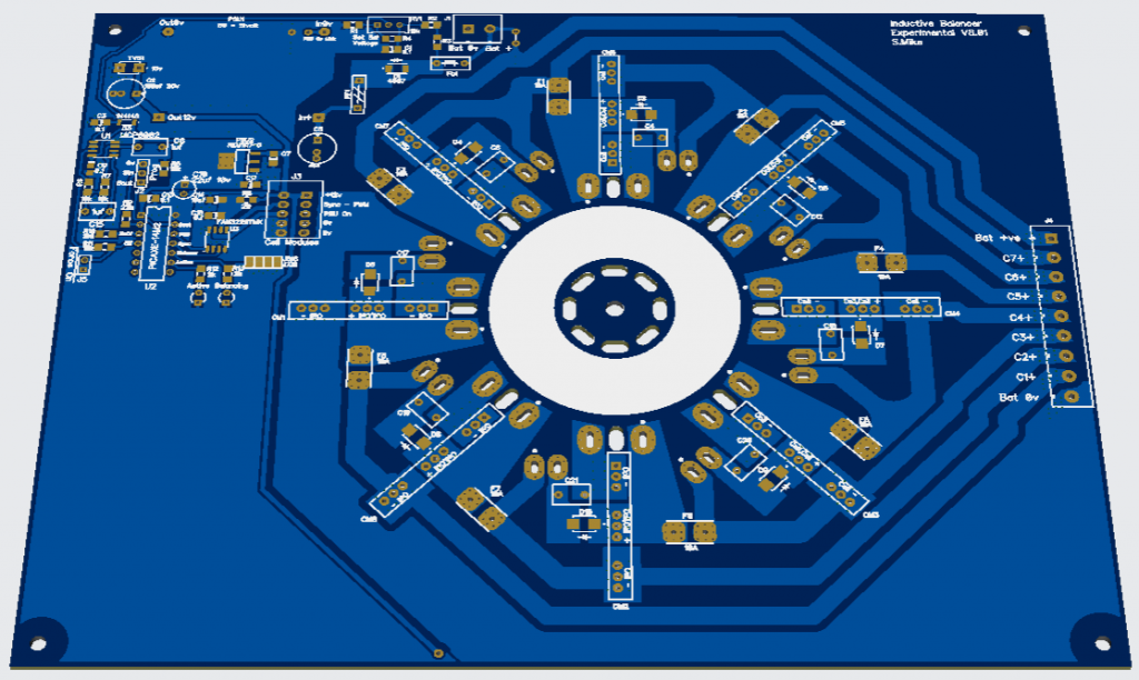
Here is the final layout for each balancer main mother board, the 8 mosfet inductor drive modules solder to the pcb, sync drive pwm connects to them by a common 10pin IDC cable; a large 63 x 35 x 25mm ferrite core sits in the center, held in place by the coil windings. To keep wiring resistances down I have opted to use copper pour planes with high current XT60 connectors so 2.5-4mm wires can be wired to each cell. Automotive type fuses are used as they have a low resistance.
Yet to make a simple driver pcb to drive the 8 modules on the main board, will use a variation of the previous one using a Picaxe.
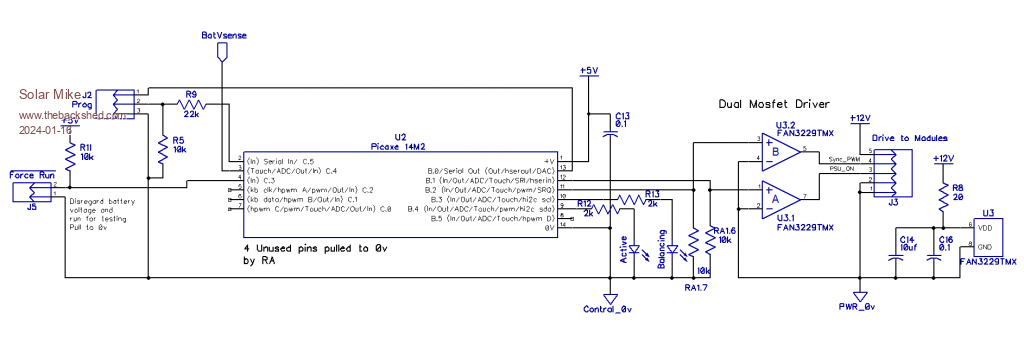
Basic schematic each balancer component:
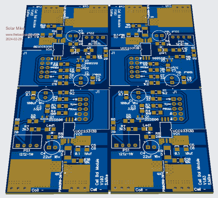
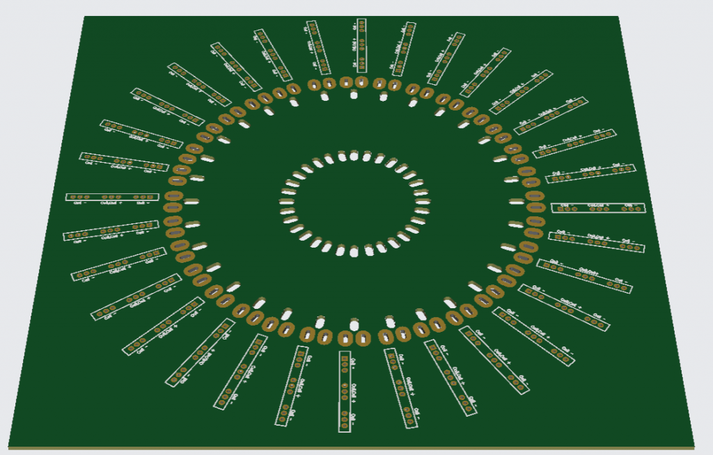
Cell modules 50 x 40mm:(4 fit on a 100x100 pcb)
Main Mother Board 171 x 171mm:
Cheers Mike
Solar Mike Guru Joined: 08/02/2015 Location: New ZealandPosts: 1124
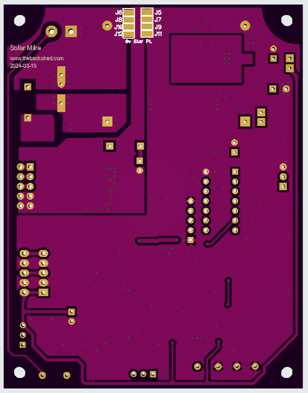
Posted: 01:23am 10 Mar 2024
Copy link to clipboard
Print this post
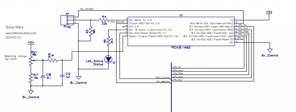
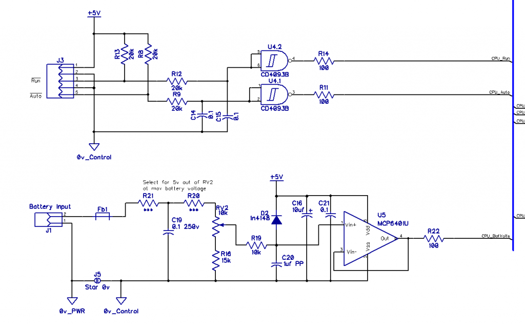
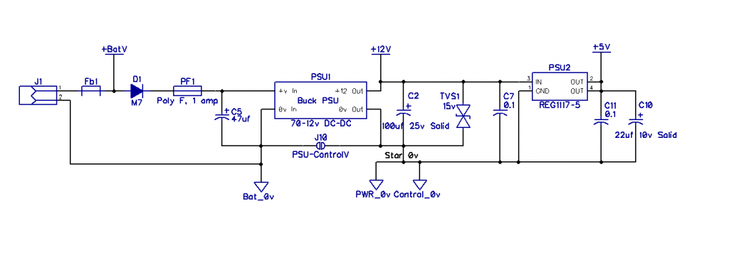
Power pcb's will get here next week; meanwhile have completed the cpu driver board, 78 x 100mm, it connects to the multiple cell interface boards linking each battery cell to the big ferrite conductor. I want to connect it to 3 x 48 volt banks of 6V lead carbon battery cells.
Have used the old Picaxe 14M2, basically it compares the 48V battery to a set point and turns on the sync pwm to the cell modules. Have allowed for a couple of switch contacts to switch to Auto or Forced run. The Forced run input could be connected to a BMS.
Some of the earlier blowups in the past were caused by the cpu outputting spurious PWM as its supply volts were powered down; to prevent this I have used a CPU reset chip, MCP100T-475, its output is normally logic high, dropping to Low if the 5v rail drops below 4.75 volts. This output feeds a NAND gate input and turns off both module driver outputs before the CPU PWM goes ballistic.
I will be eventually driving 32 Lifepo4 cell modules for my 100V bank, so have used a 12V mosfet driver chip for the two main outputs to supply enough drive current.
Schematic below, note I haven't shown the 12 and 5V supplies.
PCB:
Cheers Mike
Solar Mike Guru Joined: 08/02/2015 Location: New ZealandPosts: 1124
Posted: 09:44am 06 Apr 2024
Copy link to clipboard
Print this post
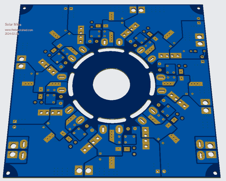
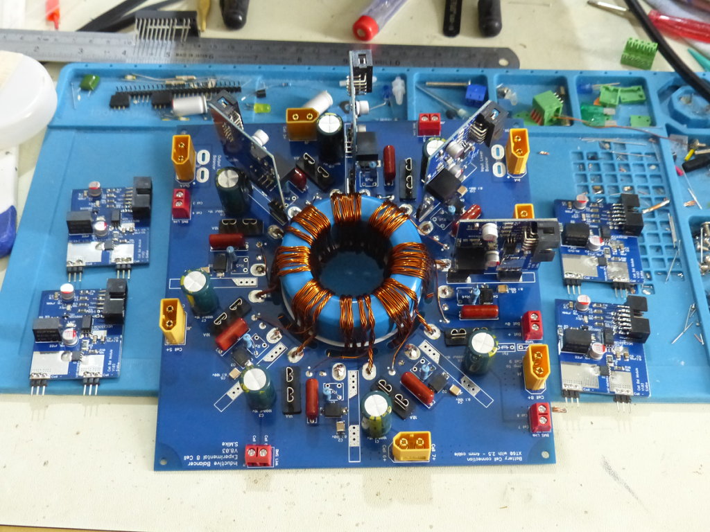
Spent some more time on this project, here is a photo of the 8-cell host pcb containing the large central ferrite core and 8 bifilar windings; each paired winding is 4 turns of 5 strand 0.56mm wire + 4 turns of single strand for the energy recovery core reset. Drive is 20Khz 50% duty.
The little synchronous switching power boards for each winding are soldered to the main pcb (for testing have wired four to sockets, so can be easily removed). A 10 pin ribbon cable runs around the outside with the 12v supply and drive signals. XT60 connectors are used for robust connections back to each cell in the bank, will do my initial tests on a 24v bank of 6v lead acid batteries, eventually these boards will be used on three 48v banks (each 8 x 6v in series).
The theory is as all power boards are turned on synchronously driving the shared core, effectively place all cells in a virtual parallel connection, so any higher voltage cell will transfer energy to lower voltage cells; ie all voltages will tend to equalize.
It worked pretty well on my initial 2 cell setup, but remains to be seen how well this will work.


 .
.