|

|
Forum Index : Microcontroller and PC projects : Sprint Layout PCB software
| Author | Message | ||||
| Rickard5 Guru Joined: 31/03/2022 Location: United StatesPosts: 463 |
Does anyone here still Use Sprint Layout 6.0? I bought a while back and never learned it, and once again my Ambition has way outstripped my Ability! But I really need to be able to Generate PCB Gerbber files for my 3018 desk top mill so I can make some PCBs that would cost way too much to farm out Sorry I'm just frustrated with sprint, I should be able to import a DXF from Autocad, and every tutorial I found on Youtube Sucks, I did the KiCad workshop a couple weeks ago at the Vintage Computer Festival and that was like a bad drunk thanks I may be Vulgar, but , while I'm poor, I'm Industrious, Honest, and trustworthy! I Know my Place |
||||
| Mixtel90 Guru Joined: 05/10/2019 Location: United KingdomPosts: 8778 |
No, Sprint Layout can't import or export DXF files. You can load a BMP file but it comes in as an image. You can then trace over it. You can also import Gerber files but they are exploded into primitives. Sprint Layout is very easy to use and making the Gerber and DRL files from your design is a piece of cake. . Edited 2024-07-17 02:15 by Mixtel90 Mick Zilog Inside! nascom.info for Nascom & Gemini Preliminary MMBasic docs & my PCB designs |
||||
| Andy-g0poy Regular Member Joined: 07/03/2023 Location: United KingdomPosts: 85 |
Do you have a different way to generate the isolation routing gerber files? If so I would suggest you try one of the many different PCB layout programs. I use Kicad which is free, and normally send the files off to jclpcb to make the PCB it's very cheap. However and this applies to ALL cad software programs, there is a steep learning curve, and you cannot expect to dive right in and produce a complex layout. You need to take the time and run through the tutorials and get to know the software. (Whatever it is) Almost all PCB software needs a full circuit diagram to generate a valid netlist. So importing just a track layout is not a common function, and usually causes more issues than it's worth. Many people find Kicad difficult, but that's just because it works in a slightly different way to most other PCB design software, (in particular eagle) You just have to get used to it. Andy |
||||
| Mixtel90 Guru Joined: 05/10/2019 Location: United KingdomPosts: 8778 |
For PCB design you can't go far wrong with EasyEDA (free and less of a learning curve than KiCAD IMHO), but it looks like Rick is definitely looking for a way to produce gerber files for a milling machine rather than etching. I think that might require more specific control. It all depends on his design. SL6 is designed as a "free drawing" program. You can draw just about anything to 0.001mm. It doesn't require input from a circuit diagram. Mick Zilog Inside! nascom.info for Nascom & Gemini Preliminary MMBasic docs & my PCB designs |
||||
| PhenixRising Guru Joined: 07/11/2023 Location: United KingdomPosts: 1855 |
I think Mick will agree; spend a little time with SL6 and the darned thing sucks you in and puts a big 'ol smile on your face. We are basically tying together pre-built MCU modules with signal conditioning devices and so it's more like joining-the-dots. Even if SL6 had a great auto-router, I wouldn't use it. Once one masters the interaction of the SPACE bar and the mouse, drawing beautifully aligned tracks is easy and in my case, enjoyable. I don't have the greatest of patience to learn how to use apps but this thing just does what you want it to do.  Edited 2024-07-17 08:43 by PhenixRising |
||||
Grogster Admin Group Joined: 31/12/2012 Location: New ZealandPosts: 9936 |
I've been using SL since version 4!  I do ALL my boards on it, and that is now hundreds and hundreds of designs. PCB software is something of a personal choice, I have found. It is also HOTLY debated - the pros and cons of one over the other.  SL6 has it's limitations, but it is very easy to use and learn. SL6 does not have many of the more advanced features of the bigger packages, but I have always found it does what I need and has never let me down. SL6 has the DISADVANTAGE that it is limited to four-layer, and is Windoze only. They don't have a Linux version, and when I asked, they told me they were never planning to do a Linux port. Many other PCB design programs are multi-platform now, and you can run them on Windoze, MAC or Linux. So, there is that. One thing I lament semi-regularily, is that I would be on Linux 24/7 now and not on Windoze anymore, if SL6 was released in a Linux version. Various attempts to force SL6 onto Linux via WINE or a VM etc, have been either unsuccessful/unstable or just a pain in the bum to get it to interact with the Linux system. Installing SL6 inside a VM works very well on Linux, but if you have to run a VM Windoze, you might as well just run Windoze. MHOO - I realize this ALSO is a bit of a hot topic for debate!  But, I digress.... Smoke makes things work. When the smoke gets out, it stops! |
||||
| Mixtel90 Guru Joined: 05/10/2019 Location: United KingdomPosts: 8778 |
The main niggles I have with SL6 are: There is no comments layer. You can't even use internal layers for comments as any lines on them short out the traces on the other layers! It needs an extra layer that works like O, which has no effect on the traces but is also not an outline/cutting layer. Such a layer would not be included in the gerbers normally. Vias are pads, not vias in their own right. They shouldn't be treated in the same way. A via with or without solder mask or covered in silkscreen is not an error. You can't import/export DXF - the most common CAD format in the world. Actually, considering that those are my major niggles it's an excellent program. :) Pity there's no Linux version. It's one of those applications that I think would do very well on there. @Rick - You do need to spend some time playing with SL6 to find your way around. Like all technical software you can't just dive in and produce perfect results in 10mins. If you think this is bad then never even glance at KiCAD, The Gimp, Photoshop or the full AutoCAD package. :) ---------- I do have a problem at the moment though. Sometimes when I save a Macro it saves it mirrored horizontally on the back of the board. I must be doing something stupid, or is it Windows? Mick Zilog Inside! nascom.info for Nascom & Gemini Preliminary MMBasic docs & my PCB designs |
||||
Grogster Admin Group Joined: 31/12/2012 Location: New ZealandPosts: 9936 |
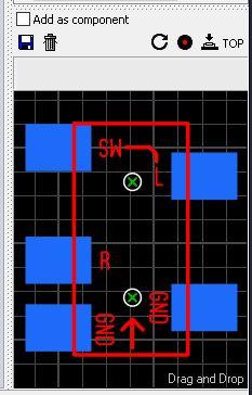
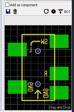
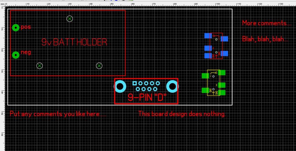
@ Mick - use the "TOP" button, in the macro preview window. Perhaps you have clicked that, which would make the macro save as though it needs to be on the bottom side of the board.   For comments, I just make the windows size LARGER then the outline, and put my comments on that. They never end up on the board in any way(being outside the board outline), and can even serve to give instructions to the PCB house.  I'm with you on the DXF support, or lack thereof. I wish they would add that. Smoke makes things work. When the smoke gets out, it stops! |
||||
| PhenixRising Guru Joined: 07/11/2023 Location: United KingdomPosts: 1855 |
"This board design does nothing" Hey, I've had that same problem  |
||||
Grogster Admin Group Joined: 31/12/2012 Location: New ZealandPosts: 9936 |
    Smoke makes things work. When the smoke gets out, it stops! |
||||
| Mixtel90 Guru Joined: 05/10/2019 Location: United KingdomPosts: 8778 |
Thanks Grogster, I'll check that out. :) Yep, comments are fine outside the outline, they simply crop the board there. Everything inside the outline goes through the DRC and goes on the gerbers though. That means that any comments there have to be on a silkscreen or the outline layer and you have to delete them (not just switch them off) when you get the board made. You can't leave comments there for next time you want to look at the board. Mick Zilog Inside! nascom.info for Nascom & Gemini Preliminary MMBasic docs & my PCB designs |
||||
| phil99 Guru Joined: 11/02/2018 Location: AustraliaPosts: 3163 |
A possible work-around, create a fake component whose name is the comment. Eg the "9V-Bat Holder" outline on your Does Nothing board could contain a reasonable amount of text. |
||||
| v.lenzer Senior Member Joined: 04/05/2024 Location: GermanyPosts: 106 |
If you just want to save a comment or description about the project, you can use "Project Info" under "Tools"("Extras" in the german version. Best wishes! Joachim |
||||
| asknik2022 Regular Member Joined: 26/03/2022 Location: United KingdomPosts: 94 |
I use the free version of Dip Trace Export to Gerber files and then use Flatcam and import Gerber files to create the CNC File for the CNC Machine. I used to do this all the time on the CNC 3018 with a 0.15-0.20 15% V-Bit etc. until I found out that I can get 5 PCBS made in China for $5 + $6-$8 shipping, takes about 10 days to arrive in UK. |
||||
| Rickard5 Guru Joined: 31/03/2022 Location: United StatesPosts: 463 |
I have been using JLB pcb up til now , but I want to try PCB Way for 10 for $5, and as Always I Buy Visa gift cards when doing anything with China ! My end goal to use the PCB as Mechanical Part and circuit Board Like I have a design in my Mind of a Robot Arm where the flat planes of the arm are also the Picomite and the Support Circuitry. I'm also Kinda weirdly in too Sumo Robots and it would be really cool to do the same thing :) My goal is to be able to order my 10 or what ever boards and when they come in, be able to Fixture them in to my 3018 and profile cut the parts. I may be Vulgar, but , while I'm poor, I'm Industrious, Honest, and trustworthy! I Know my Place |
||||
| PhenixRising Guru Joined: 07/11/2023 Location: United KingdomPosts: 1855 |
PayPal is the way to go.  I have just purchased a lot of stuff from AliExpress and it has been an absolute pleasure. They often state "delivery within seven days". Sometimes it takes eight days and they automatically credit me with £1 "late fee". There was one item that was taking an unreasonable amount of time to even be dispatched. I cancelled that item and AE immediately informed me that they were refunding me. A few hours later, I received a notification from PayPal stating that I'd received the refund.   |
||||
| Mixtel90 Guru Joined: 05/10/2019 Location: United KingdomPosts: 8778 |
Same here. I use PayPal all the time now because it hides your bank details from the seller. They also get paid immediately so there's no hold-up in getting your order processed. AE have a £1 credit waiting for me at the moment because my order took 8 days. :) Mick Zilog Inside! nascom.info for Nascom & Gemini Preliminary MMBasic docs & my PCB designs |
||||
| pwillard Guru Joined: 07/06/2022 Location: United StatesPosts: 339 |
Sprint Layout is my goto software for anything small and easy to work out. Its so simple to whip up a part from datasheet specs. Way easier than KICAD, but then its whole purpose was to easily whip up a new PCB. Its easy to learn and the Gerber output is accepted by JLCPCB so no reason to grab KICAD unless the project has more than 30 parts or so. |
||||
| The Back Shed's forum code is written, and hosted, in Australia. | © JAQ Software 2026 |