|

|
Forum Index : Microcontroller and PC projects : One for matherp - JLC question about CMM2 layers...
| Author | Message | ||||
Grogster Admin Group Joined: 31/12/2012 Location: New ZealandPosts: 9936 |
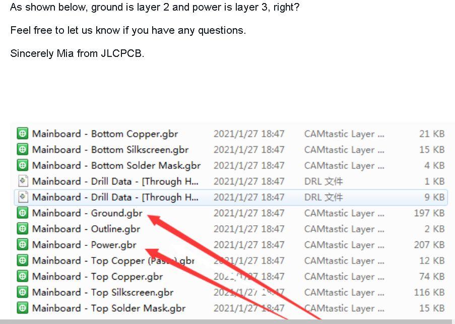
I've never been asked this before, even though I got heaps of CMM2 boards from JLC prior to the virus, but this tech wants to know about the ground and power plane layers - Peter, please advise....  Smoke makes things work. When the smoke gets out, it stops! |
||||
| matherp Guru Joined: 11/12/2012 Location: United KingdomPosts: 11250 |
top,ground,power,bottom is correct |
||||
Grogster Admin Group Joined: 31/12/2012 Location: New ZealandPosts: 9936 |
Thanks. Not sure why they asked about this, as in the past....... Smoke makes things work. When the smoke gets out, it stops! |
||||
| Mixtel90 Guru Joined: 05/10/2019 Location: United KingdomPosts: 8781 |
That list is almost as if it's for a multi-layer board. I'd have expected "Top Copper" and "Bottom Copper" to be the layers populated. Perhaps it is? I don't know. Mick Zilog Inside! nascom.info for Nascom & Gemini Preliminary MMBasic docs & my PCB designs |
||||
Grogster Admin Group Joined: 31/12/2012 Location: New ZealandPosts: 9936 |
The G2 is a four-layer, from what I can see. Top and Bottom copper are the outside top and bottom layers, and "Ground" and "Power" are internal ground and power plane layers, so JLC were just wanting to make sure they got the power and ground layers the right way around. Still, it's odd - I must have got JLC to make heaps of assembled boards before the virus slowed the planet to a crawl, and they never asked that question before. Oh well. Smoke makes things work. When the smoke gets out, it stops! |
||||
| The Back Shed's forum code is written, and hosted, in Australia. | © JAQ Software 2026 |